Minimizing degradation of SiC bipolar semiconductor devices

a technology of bipolar semiconductors and degradation minimization, which is applied in the direction of chemically reactive gases, crystal growth process, polycrystalline material growth, etc., can solve the problems of limiting the use of devices or sensors for high temperature applications, the respective band gap of silicon and gallium arsenide is too small to support the generation of certain wavelengths, and the specific limitations of silicon and gallium arsenide based semiconductors

Inactive Publication Date: 2005-06-02
SUMAKERIS JOSEPH J +6
View PDF12 Cites 19 Cited by
  • Summary
  • Abstract
  • Description
  • Claims
  • Application Information

AI Technical Summary

Problems solved by technology

Nevertheless, silicon and gallium arsenide based semiconductors have particular limitations that generally prevent them from being used to produce certain types of devices, or devices that can be used under certain operating conditions.
For example, the respective bandgaps of silicon and gallium arsenide are too small to support the generation of certain wavelengths of light in the visible or ultraviolet areas of the electromagnetic spectrum.
Similarly, silicon and gallium arsenide based devices can rarely operate at temperatures above 200° C. This effectively limits their use as devices or sensors in high temperature applications such as high power electric motor controllers, high temperature combustion engines, and similar applications.
In particular, silicon carbide has an extremely high melting point and is one of the hardest known materials in the world.
Because of its physical properties, however, silicon carbide is also relatively difficult to produce.
Because silicon carbide can grow in many polytypes, it is difficult to grow into large single crystals.
The high temperatures required to grow silicon carbide also make control of impurity levels (including doping) relatively difficult, and likewise raise difficulties in the production of thin films (e.g. epitaxial layers).
Because of its hardness, the traditional steps of slicing and polishing semiconductor wafers are more difficult with silicon carbide.
Similarly, its resistance to chemical attack and impurity diffusion makes it difficult to etch and process using conventional semiconductor fabrication techniques.
As a result, growing single crystal substrates and high quality epitaxial layers (“epilayers”) in silicon carbide has been, and remains, a difficult task.
This substantial change in forward voltage represents a problem that can prohibit the full exploitation of silicon carbide-based bipolar devices in many applications.
Although multiple defects may be responsible for the observed Vf degradation (also called Vf drift), present research indicates that one of the causes for the increase in forward voltage is the growth of planar defects such as stacking faults in the silicon carbide structure under the application of forward current in a bipolar device.
When the stacking faults progress too extensively, they tend to cause the forward voltage to increase in an undesirable manner that can prevent the device from operating as precisely as required or desired in many applications.
Other types of crystallographic defects can likewise cause degradation.
As those familiar with crystal structure and growth are well aware, perfect crystal structures are never achieved.
For these and other reasons, crystal flaws, including stacking faults, can be expected to appear even under the best of growth circumstances.

Method used


Image

  • Minimizing degradation of SiC bipolar semiconductor devices
  • Minimizing degradation of SiC bipolar semiconductor devices
  • Minimizing degradation of SiC bipolar semiconductor devices

Examples


Embodiment Construction

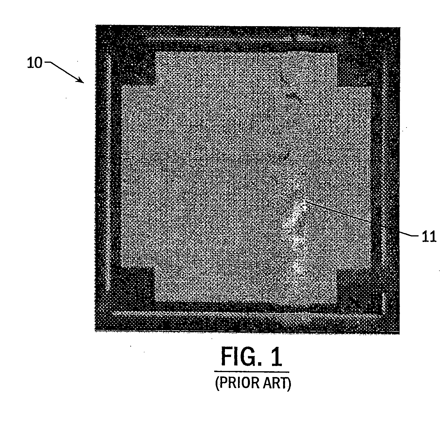
[0028]FIG. 1 is a photomicrograph of a prior art 1.2 mm×1.2 mm p-n diode broadly designated at 10. The diode depicted in plan view in FIG. 1 exhibits a patterned top side ohmic contact which permits visual inspection of the device during operation.

[0029]FIG. 1 illustrates an extensive group of stacking faults 11 that spans the entire width (vertically in the orientation of FIG. 1) of the device. Although not visible in plan view, stacking faults 11 exist in multiple atomic planes of device 10. This is typical of the type of stacking fault that grows during forward operation of the device and causes the problems referred to in the background portion of the specification. The stacking faults 11 are formed after operation of the device under forward bias conditions for 30 minutes. Regions of the stacking faults are visible in FIG. 1 because they serve as recombination centers which under some conditions produce visible light during forward bias operation due to electron-hole recombina...


PUM

PropertyMeasurementUnit
carrier concentrationaaaaaaaaaa
temperaturesaaaaaaaaaa

Abstract

A method of forming a bipolar device includes forming at least one p-type layer of single crystal silicon carbide and at least one n-type layer of single crystal silicon carbide on a substrate. Stacking faults that grow under forward operation of the device are segregated from at least one of the interfaces between the active region and the remainder of the device. The method of forming bipolar devices includes growing at least one of the epitaxial layers to a thickness greater than the minority carrier diffusion length in that layer. The method also increases the doping concentration of epitaxial layers surrounding the drift region to decrease minority carrier lifetimes therein.

Description

CROSS REFERENCE TO RELATED APPLICATIONS [0001] This application is a continuation of application Ser. No. 10 / 046,346 filed Oct. 26, 2001, for “Minimizing Degradation of SiC BiPolar Semiconductor Devices,” now U.S. Pat. No.______.STATEMENT REGARDING FEDERALLY FUNDED RESEARCH AND DEVELOPMENT [0002] This invention was developed with Government support under Government contracts F33615-01-2-2108 and F33615-00-C-5403. The Government may have certain rights in this invention.BACKGROUND OF THE INVENTION [0003] The present invention relates to increasing the quality and desired properties of semiconductor materials used in electronic devices, particularly power electronic devices. In particular, the invention relates to an improved process for minimizing crystal defects in silicon carbide, and the resulting improved structures and devices. [0004] The term “semiconductor” refers to materials whose electronic properties fall between the characteristics of those materials such as metals that a...

Claims


Application Information

Patent Timeline
Patent Type & Authority Applications(United States)
IPC IPC(8): H01L29/24H01L29/732H01L29/744H01L29/861
CPCC30B19/00C30B23/02C30B25/02C30B29/36H01L29/861H01L29/6606H01L29/66068H01L29/732H01L29/744H01L29/1608C30B23/002H01L29/73
Inventor SUMAKERIS, JOSEPH J.SINGH, RANBIRPAISLEY, MICHAEL JAMESMUELLER, STEPHAN GEORGHOBGOOD, HUDSON M.CARTER, CALVIN H. JR.BURK, ALBERT AUGUSTUS JR.
Owner SUMAKERIS JOSEPH J
Why Eureka
Try Eureka