Silicon wafer production process and silicon wafer

a production process and silicon wafer technology, applied in the direction of polycrystalline material growth, after-treatment details, under protective fluid, etc., can solve the problems of deterioration of goi, limited effect of surface vicinity, and deterioration of goi, so as to improve the product yield and improve the device characteristics and reliability, the effect of superior crystallinity

Active Publication Date: 2006-02-09
SUMITOMO MITSUBISHI SILICON CORP
View PDF1 Cites 19 Cited by
  • Summary
  • Abstract
  • Description
  • Claims
  • Application Information

AI Technical Summary

Benefits of technology

[0013] In consideration of the aforementioned problems, an object of the present invention is to provide a silicon wafer production process which can decrease detrimental effects attributable to residual crystal defects grown from defect nucleations such as oxidation induced stacking faults (OSFs that are grown from OSF nuclei) and the like and residual processing-induced defects caused by polishing and other machine work, thereby resulting in obtaining a silicon wafer having superior 001, and to provide a silicon wafer having superior GOI.
[0014] As a result of extensive studies, the inventors of the present invention found that, in a silicon wafer production process, by performing RTA treatment in hydrogen, argon or in an atmosphere containing a mixture thereof on a silicon wafer (silicon wafer free of COP defects and FPDs) that has been cut out from a perfect region (which may contain an R-OSF region (a region in which there is occurrence of ring-shaped oxidation induced stacking faults)) free of vacancy-type point defects and interstitial-type point defects, a silicon wafer can be obtained that exhibits superior improvement of surface characteristics, does not require re-polishing following rapid heating and cooling treatment to enhance oxygen precipitation, and has satisfactory GOI characteristics.

Problems solved by technology

However, although the aforementioned near-perfect crystal silicon wafer is basically free of COP defects and dislocations, residual crystal defects such as oxidation induced stacking fault nuclei (OSF nuclei) are formed due to slight changes in growth conditions, thereby resulting in the problem of the residual crystal defects causing deterioration of GOI.
Also, residual defects resulting from the wafer processing process have been determined to cause deterioration of GOI.
In the case in which beat-treating a silicon wafer in argon or other inert atmosphere or hydrogen, there is the disadvantage of the effects being limited to the vicinity of the surface.
In the case of normally used wafers having COP defects, since the internal COP defects remain even after heat treatment, there is the problem of these residual COP defects having a detrimental effect on device characteristics.
In the case in which a silicon wafer is heated at high temperature by using an electric furnace, a stress occurs in wafers, in particular in wafers measuring 300 mm in diameter, a large stress occurs, and also problems of slippage occur, thereby resulting in concerns about detrimental effect on their application.
In the case in which heat-treating a silicon wafer with RTA treatment in nitrogen or oxygen, since it is necessary to remove the nitride film or oxide film formed on the surface by machine work or chemical treatment, it couled lead to cause deterioration of GOI.
In this process, although the problem of GOI deterioration resulting from machine work is resolved, in the case of normally used wafers having COP defects, even in the case of small COP defects in the manner of nitrogen-doped crystals, the COP defects are unable to be eliminated in a short period of time, thereby preventing improvement of GOI deterioration caused by the presence of COP defects in bulk.

Method used


Image

  • Silicon wafer production process and silicon wafer
  • Silicon wafer production process and silicon wafer
  • Silicon wafer production process and silicon wafer

Examples


Embodiment Construction

[0034] As follows is a description of an embodiment of the silicon wafer production process and silicon wafer according to the present invention, with reference to the drawings.

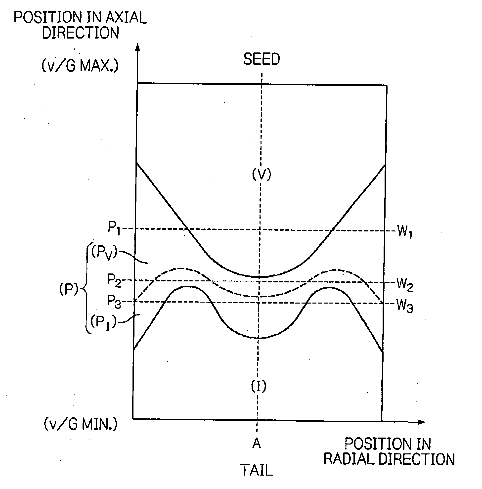
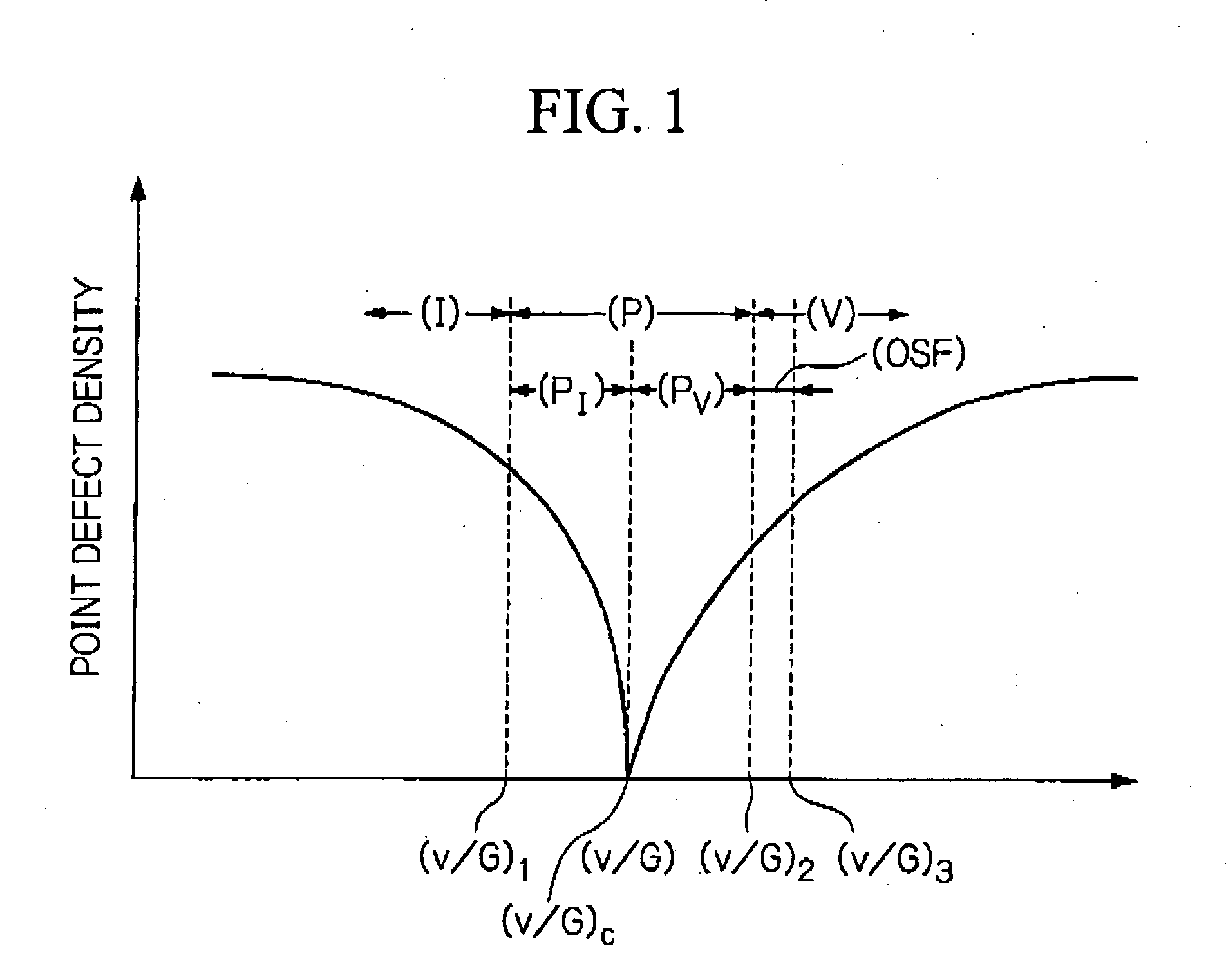
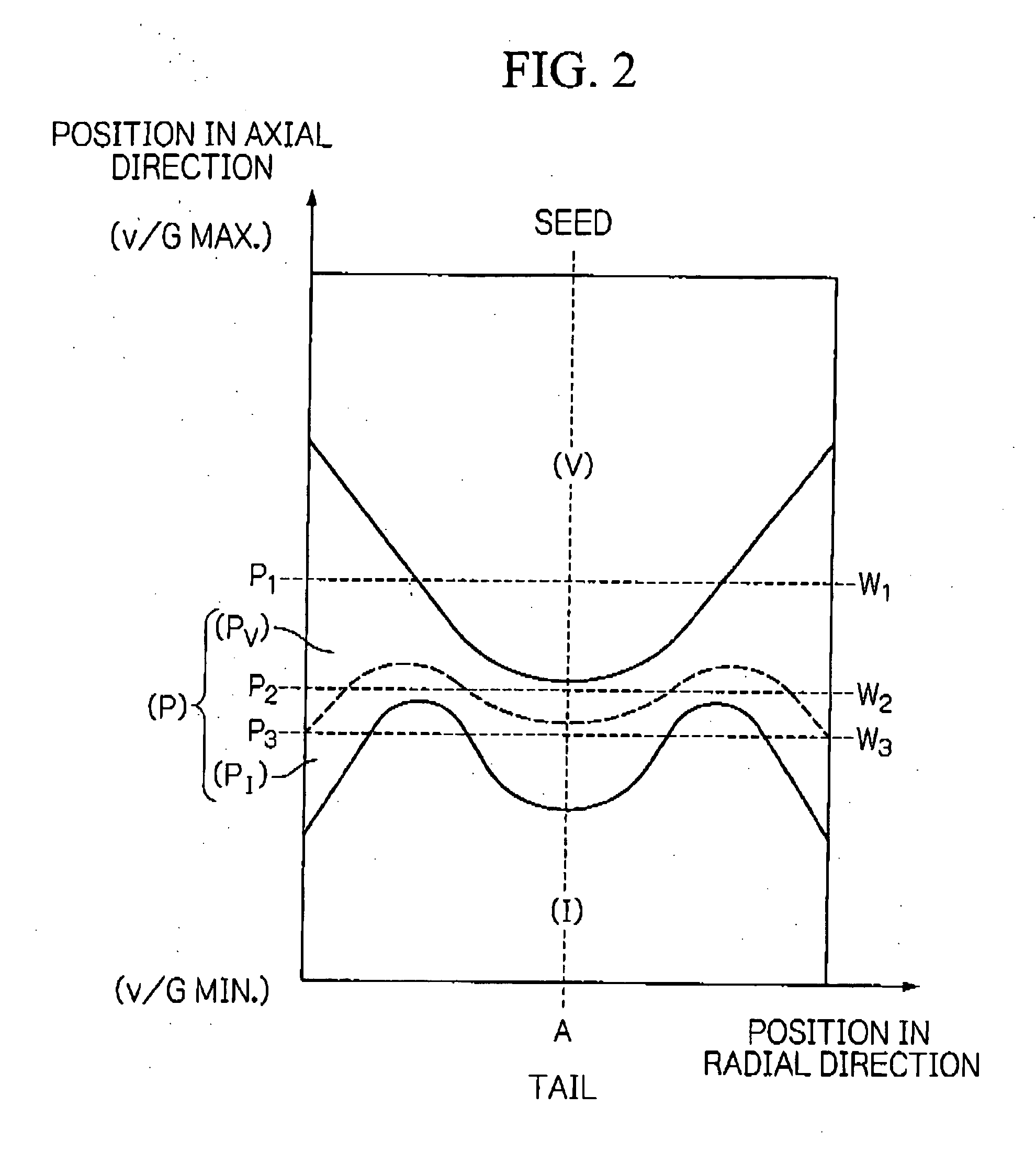
[0035] When in a silicon single crystal ingot, the region where interstitial-silicon-type point defects are predominately present is designated as region I, the region where vacancy-type point defects are predominately present is designated as region V, the perfect region where there are no agglomerates of interstitial-silicon-type point defects nor agglomerates of vacancy-type point defects is designated as perfect region P, and the region where ring-shaped oxidation induced stacking faults (R-OSF) occur is designated as region R, the embodiment of the silicon wafer production process includes a step of cutting out a silicon wafer from a silicon single crystal ingot in a perfect region which includes a perfect region P and / or a region R in which there is occurrence of R-OSF, and a step of performing rapid t...


PUM

PropertyMeasurementUnit
melting pointaaaaaaaaaa
diameteraaaaaaaaaa
temperatureaaaaaaaaaa

Abstract

This silicon wafer production process has a step of cutting a silicon wafer from a silicon single crystal ingot in a perfect region which includes a perfect region P free of agglomerates of interstitial-silicon-type point defects and agglomerates of vacancy-type point defects and / or a region R in which there is occurrence of ring-shaped oxidation induced stacking faults, and a step of performing rapid thermal annealing on the silicon wafer in a hydrogen atmosphere, an argon atmosphere or an atmosphere containing a mixed gas thereof.

Description

BACKGROUND OF THE INVENTION [0001] 1. Field of the Invention [0002] The present invention relates to a silicon wafer production process and a silicon wafer. [0003] 2. Description of the Related Art [0004] In recent years, ever since grown-in defects were demonstrated to cause deterioration of Gate Oxide Integrity (GOI) in silicon wafers, numerous attempts have been made to decrease these grown-in defects. [0005] In particular, technology for growing near-perfect crystals almost free of defects in which v / G (a ratio of ingot pulling velocity (v) to temperature gradient in the ingot near the interface between the ingot and a melt (G)) is controlled when pulling out the single crystal ingot, has been applied practically to the production process of growing near-perfect silicon single crystals. [0006] Silicon wafers free of crystal defects such as Crystal Originated Particle (COP) defects, void defects such as Flow Pattern Defects (FPDs) or the like, and dislocations and the like are us...

Claims


Application Information

Patent Timeline
Patent Type & Authority Applications(United States)
IPC IPC(8): C30B15/00C30B28/10C30B21/06C30B27/02C30B30/04
CPCC30B29/06H01L21/3225H01L21/28167C30B33/00
Inventor SHIBAYAMA, TAKASHIMURAKAMI, YOSHIOSHINGYOJI, TAKAYUKI
Owner SUMITOMO MITSUBISHI SILICON CORP
Why Eureka
Try Eureka