Seed crystal of silicon carbide single crystal and method for producing ingot using same

a technology of seed crystal, which is applied in the direction of crystal growth process, polycrystalline material growth, and polycrystalline material growth, can solve the problems of inability to stably and stably supply a large size and high-quality silicon carbide single crystal in an industrial scale, and the practical application of this material has been hindered, so as to achieve less defects

Inactive Publication Date: 2005-07-28
NIPPON STEEL CORP
View PDF2 Cites 19 Cited by
  • Summary
  • Abstract
  • Description
  • Claims
  • Application Information

AI Technical Summary

Benefits of technology

[0020] An object of the present invention is to provide a seed crystal which is capable to produce materials having less defects and a diameter suitable for practical application, and made of a silicon carbide single crystal, and a method for producing a silicon carbide single crystal ingot, a silicon carbide single crystal ingot, a silicon carbide single crystal wafer, a silicon carbide single crystal epitaxial substrate, a substrate for growing a silicon carbide single crystal epitaxial thin film (single crystal substrate), and a method of producing a silicon carbide single crystal epitaxial substrate.

Problems solved by technology

However, a crystal-growing technology capable to supply a large size and high-quality silicon carbide single crystal in an industrial scale and stably has not been established yet.
Therefore, though silicon carbide is material for a semiconductor having many merits and possibilities as described above, practical application of this material has been hindered.
However, with this method, the size of obtained single crystal is small and it is difficult to control the size and shape with a high degree of precision.
Besides, it is not easy to control crystal polymorphism and impurity-carrier concentration of silicon carbide.
Though a large size single crystal can be obtained with this method, only a silicon carbide single crystal containing many defects (up to 107 defects / cm2) due to existence of as much as about 20% of lattice mismatch with a substrate, and so on, and it is not easy to obtain a high-quality silicon carbide single crystal.
Further, a device produced on a micropipe is known that its characteristics are deteriorated (T. Kimoto et al., IEEE Tran. Electron. Device, vol.
Accordingly, reduction of the micropipe defects is one of the most important problems in device application of a silicon carbide single crystal.
Hei 5-262599, though generation of micropipe defects can be suppressed, a plenty of stacking faults causing unfavorable effect to devices are generated.

Method used


Image

  • Seed crystal of silicon carbide single crystal and method for producing ingot using same
  • Seed crystal of silicon carbide single crystal and method for producing ingot using same
  • Seed crystal of silicon carbide single crystal and method for producing ingot using same

Examples


first embodiment

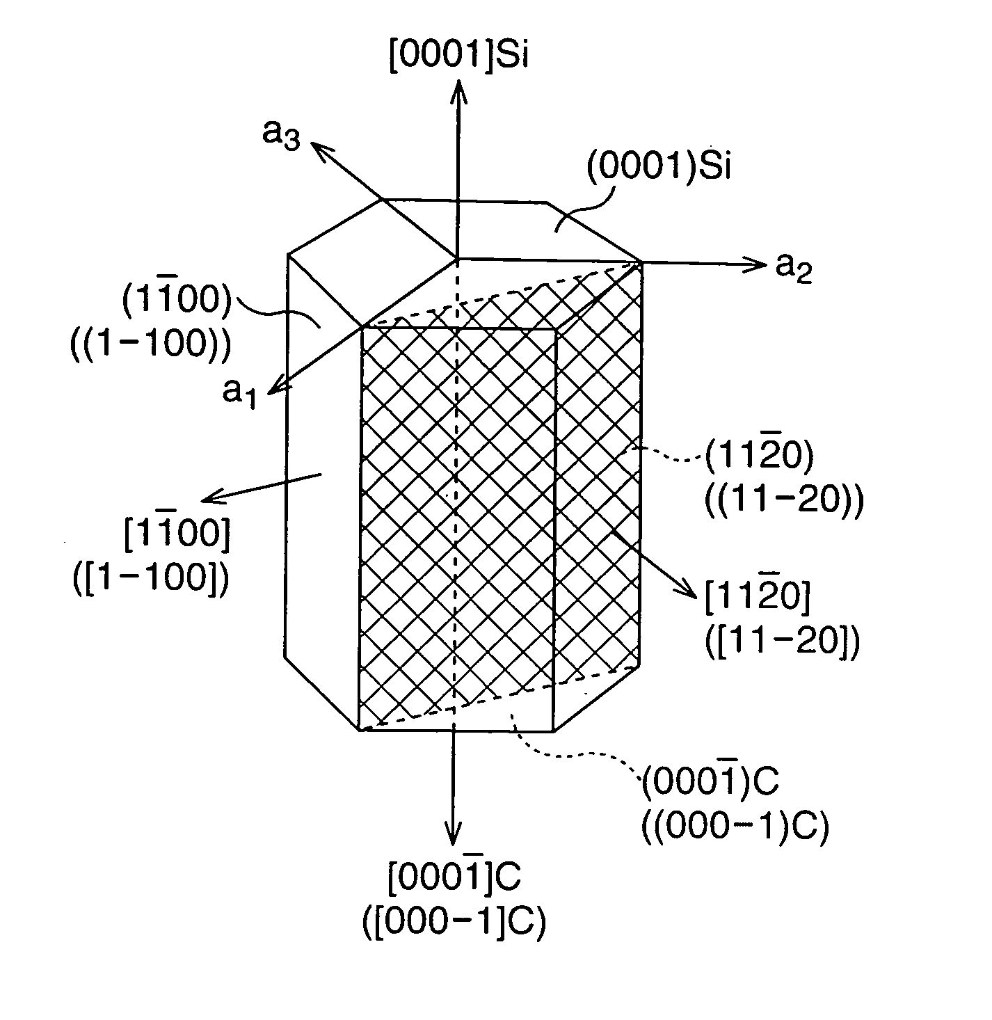
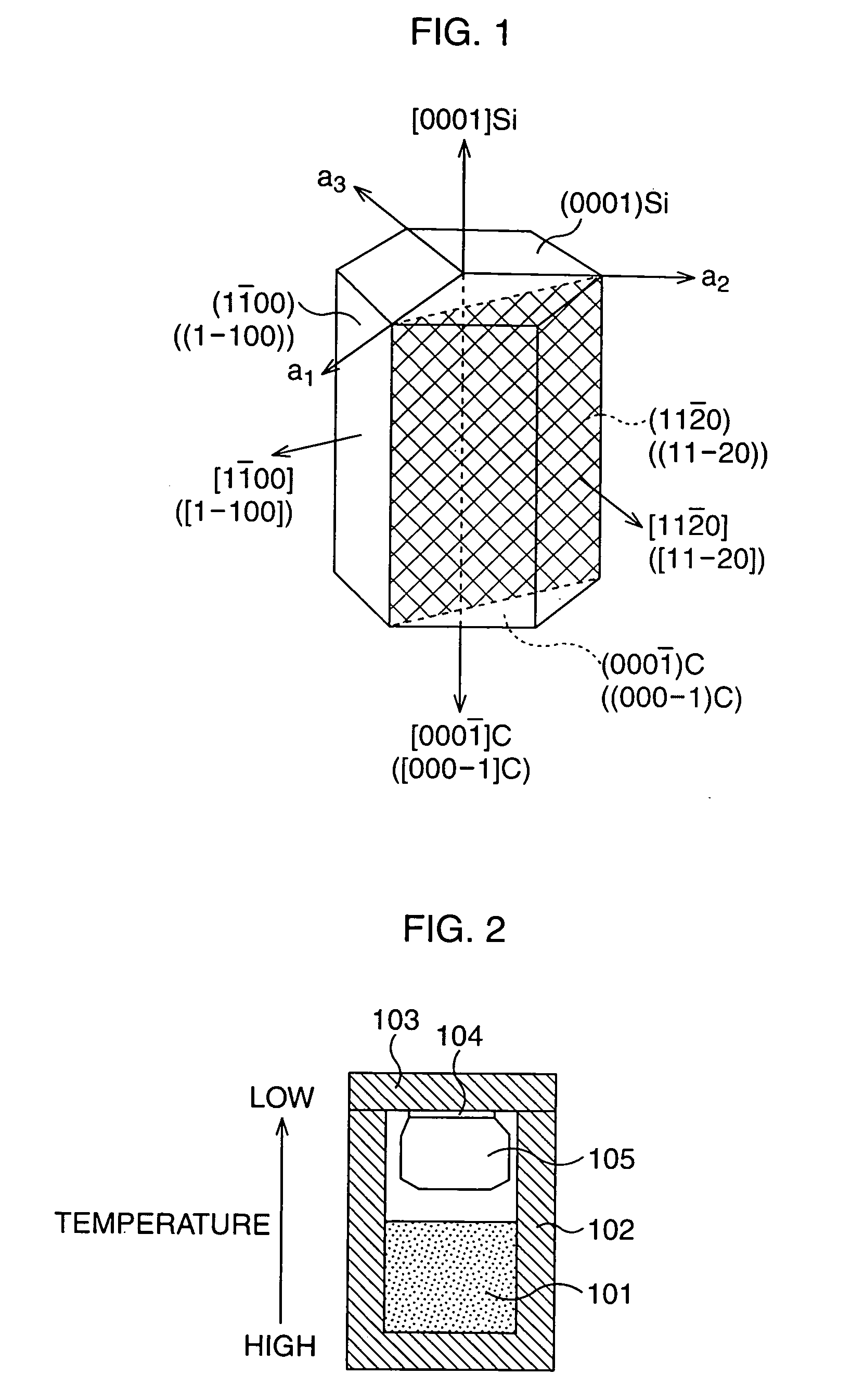
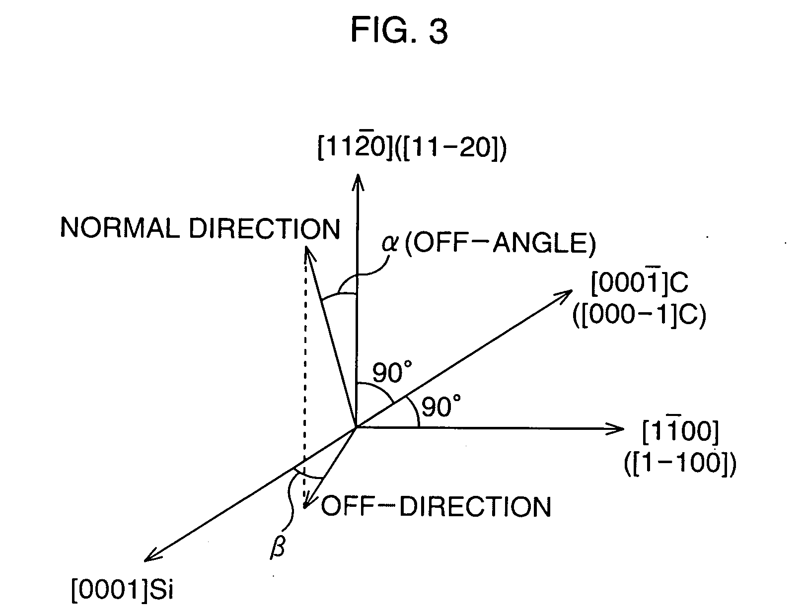
[0086] Silicon carbide single crystal was produced using a crystal growth system shown in FIG. 6. Specifically, a wafer was cut from a 6H-type silicon carbide single crystal which had grown in the [000-1] C direction. At this time, a silicon carbide single crystal which included micropipe defects but no stacking fault was used. Regarding the cut face, a face inclined at an angle of 10 degrees to the [0001] Si direction with respect to the (11-20) face of the silicon carbide single crystal was taken as the cut face (α=10°, β=0°). Incidentally, the deviation of the off-direction from the [0001] Si direction was set to be within ±1°.

[0087] And, a silicon carbide seed crystal 1 was obtained by mirror-like polishing the cut wafer. The diameter measured at this time was 20 mm at the smallest.

[0088] Thereafter, the seed crystal 1 was fixed on the inside surface of a lid 4 of a graphite crucible 3. A raw material 2 was placed in the graphite crucible 3. Then, the graphite crucible 3 fille...

second embodiment

[0096] Using a crystal growth system shown in FIG. 6, a silicon carbide single crystal was produced. Specifically, first, a wafer was cut from a 4H-type silicon carbide single crystal which had grown in the [000-1] C direction. At this time, a silicon carbide single crystal which included micropipe but no stacking faults was used. Regarding the cut face, a face inclined at an angle of 10 degrees with respect to the (11-20) face of the silicon carbide single crystal to the [000-1] C direction was taken as the cut face (α=10°, β=180°). Incidentally, the deviation of the off-direction from the [000-1] C direction was set to be within ±1°.

[0097] Then, a silicon carbide seed crystal was obtained by mirror-like polishing the cut wafer. The diameter measured at this time was 20 mm at the smallest.

[0098] Thereafter, the crystal was allowed to grow similarly to the first embodiment. As a result, the diameter of the obtained crystal was 22 mm and the height was about 16 mm.

[0099] By analyz...

third embodiment

[0104] Using the crystal growth system shown in FIG. 6, a silicon carbide single crystal was produced. Specifically, first, a wafer was cut from a 4H-type silicon carbide single crystal which had grown in the [000-1] C direction. At this time, the silicon carbide single crystal in which micropipe defects were contained but no stacking faults existed was used. Regarding the cut face, a face inclined at an angle of 10 degrees with respect to the (11-20) face of the silicon carbide single crystal in the [0001] Si direction was taken as the cut face (α=10°, β=0°). Incidentally, the deviation of the off-direction from the [000-1]Si direction was set to be within ±1°.

[0105] Then, a silicon carbide seed crystal was obtained by mirror-like polishing the cut wafer. The diameter measured at this time was 20 mm at the smallest.

[0106] Thereafter, the crystal was allowed to grow similarly to the first embodiment. However, the growth rate was set to 0.75 mm / sec. As a result, the diameter of the...


PUM

PropertyMeasurementUnit
angleaaaaaaaaaa
angleaaaaaaaaaa
angleaaaaaaaaaa

Abstract

The present invention relates to a seed crystal consisting of a silicon carbide single crystal suitable for producing a substrate (wafer) for an electric power device, a high-frequency device or the like, and a method for producing an ingot using the same. A single crystal growing face of a seed crystal consisting of a silicon carbide single crystal is inclined at an angle ranging from 3 degrees or more to 60 degrees or less with respect to the (11-20) face to a direction inclined at an angle ranging from −45 degrees or more to 45 degrees or less from a <0001> direction to the [1-100] direction. By performing crystal growth using such a seed crystal, a high quality silicon carbide single crystal ingot can be obtained. According to the present invention, it is possible to obtain material consisting of a silicon carbide single crystal of favorable quality, which has few crystal defects such as micropipe defects and stacking faults, and the diameter is suitable for practical application.

Description

TECHNICAL FIELD [0001] The present invention relates to a seed crystal consisting of a silicon carbide single crystal suitable for producing a substrate (wafer) for an electric power device, a high-frequency device or the like, and a method for producing an ingot using the same. BACKGROUND ART [0002] Silicon carbide (SiC) has attracted a great deal of attention as material for an environmental resistance semiconductor because of its physical and chemical properties such as excellent in heat resistance and mechanical strength, durability against radiation, and the like. Further, in recent years, demand for a silicon carbide single crystal wafer as a substrate wafer for a short wavelength optical device from blue to ultra violet light, a high-frequency high blocking voltage electron device, and the like has been increased. However, a crystal-growing technology capable to supply a large size and high-quality silicon carbide single crystal in an industrial scale and stably has not been ...

Claims


Application Information

Patent Timeline
Patent Type & Authority Applications(United States)
IPC IPC(8): C30B23/00C30B25/00C30B25/20
CPCC30B25/00C30B25/20C30B23/005C30B23/00C30B29/36
Inventor OHTANI, NOBORUKATSUNO, MASAKAZUFUJIMOTO, TATSUO
Owner NIPPON STEEL CORP
Why Eureka
Try Eureka