Three-dimensional quantum well transistor and fabrication method

a three-dimensional quantum well and transistor technology, applied in the field of semiconductor technology, can solve the problems of high resistance in the channel region, serious affecting device performance, and non-uniform density of two-dimensional electron gas in the channel

Active Publication Date: 2014-07-24
SEMICON MFG INT (SHANGHAI) CORP
View PDF1 Cites 42 Cited by
  • Summary
  • Abstract
  • Description
  • Claims
  • Application Information

AI Technical Summary

Problems solved by technology

As dimensions of semiconductor devices continue to shrink, short-channel effect may seriously affect device performance.
For HEMTs, however, the gate may have less or weak control on the extended area of the channel re...

Method used


Image

  • Three-dimensional quantum well transistor and fabrication method
  • Three-dimensional quantum well transistor and fabrication method
  • Three-dimensional quantum well transistor and fabrication method

Examples


Embodiment Construction

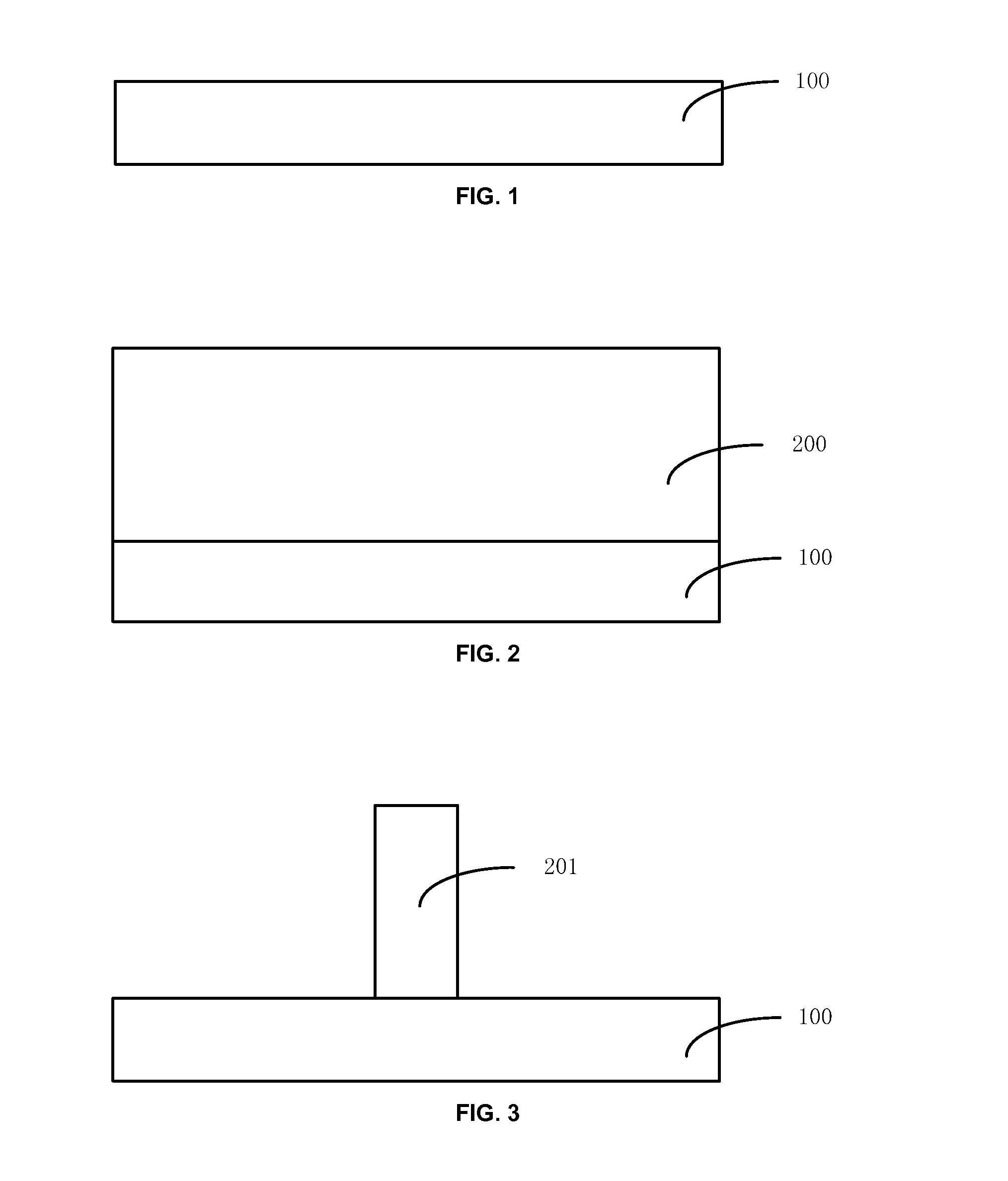
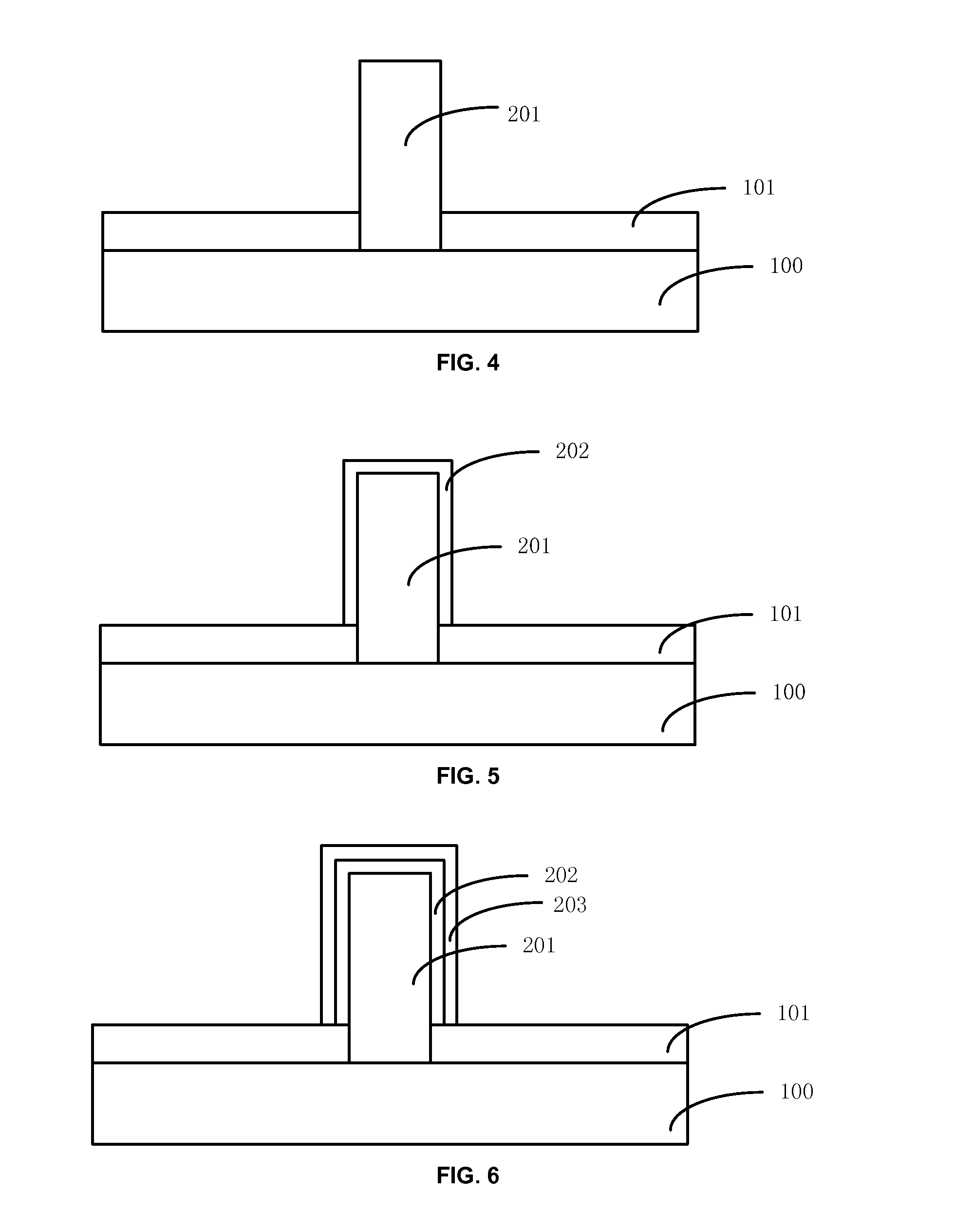
[0012]Reference will now be made in detail to exemplary embodiments of the disclosure, which are illustrated in the accompanying drawings. Wherever possible, the same reference numbers will be used throughout the drawings to refer to the same or like parts.

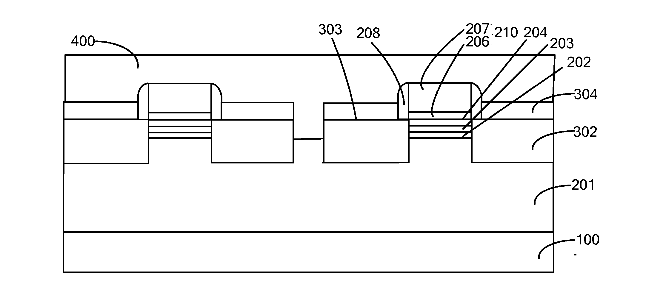
[0013]Three-dimensional quantum well (3D-QW) transistors and methods of forming the 3D-QW transistors are provided. On an insulating surface of a fin part formed from a buffer layer, a QW layer, a barrier layer, and a gate structure can be sequentially formed. The gate structure can be formed on the barrier layer and across the fin part. The QW layer and the barrier layer can form a hetero-junction of the transistor across the fin part. The disclosed transistors and fabrication methods can reduce resistance of the transistor channel region, improve the source-drain current, and increase the thermal stability of the transistor.

[0014]FIG. 23 depicts a flowchart of an exemplary method for forming a transistor consistent with the disc...


PUM


Abstract

Three dimensional quantum well transistors and fabrication methods are provided. A quantum well layer, a barrier layer, and a gate structure can be sequentially formed on an insulating surface of a fin part. The gate structure can be formed over the barrier layer and across the fin part. The QW layer and the barrier layer can form a hetero-junction of the transistor. A recess can be formed in the fin part on both sides of the gate structure to suspend a sidewall spacer. A source and a drain can be formed by growing an epitaxial material in the recess and the sidewall spacer formed on both sidewalls of the gate electrode can be positioned on surface of the source and the drain.

Description

CROSS-REFERENCES TO RELATED APPLICATIONS[0001]This application claims priority to Chinese Patent Application No. 201310024090.3, filed on Jan. 22, 2013, the entire contents of which are incorporated herein by reference.FIELD OF THE DISCLOSURE[0002]The present disclosure relates to the field of semiconductor technology and, more particularly, relates to three-dimensional quantum well (3D-QW) transistors and fabrication methods.BACKGROUND[0003]In a typical MOS device, a channel region is formed by doping the semiconductor substrate with impurities. The channel region may have both majority carriers and ionized impurities. The majority carriers may be scattered by the ionized impurities during a migration process. The mobility of carriers and the device performance can be reduced. As dimensions of semiconductor devices continue to shrink, short-channel effect may seriously affect device performance.[0004]High electron mobility transistors (HEMTs) have a channel region formed by a heter...

Claims


Application Information

Patent Timeline
IPC IPC(8): H01L29/78H01L29/15H01L29/267H01L29/66
CPCH01L29/66431H01L29/151H01L29/785H01L29/66795H01L29/267H01L29/0657H01L29/0665H01L29/1054H01L29/2003H01L29/201H01L29/205H01L29/517H01L29/66462H01L29/7783H01L29/7789
Inventor XIAO, DE, YUAN
Owner SEMICON MFG INT (SHANGHAI) CORP
Why Eureka
Try Eureka