Luminescence display apparatus and method for fabricating the same

a technology of luminescence display and display apparatus, which is applied in the direction of luminescence screen, discharge tube, instruments, etc., can solve the problems of reducing the contrast ratio of applied products, reducing the photo leakage current generated, and pixel defects, so as to reduce the photo leakage of tft due to self-emitted light, excellent gradation controllability, and less defects

Inactive Publication Date: 2005-08-04
NEC CORP
View PDF3 Cites 43 Cited by
  • Summary
  • Abstract
  • Description
  • Claims
  • Application Information

AI Technical Summary

Benefits of technology

[0026] In accordance with the present invention, the light emitted from the EL device in its own structure and reflected on the substrate or the interlayer film can be attenuated before reaching the TFT by using the light blocking structure. Accordingly, the photo leakage of the TFT due to the self-emitted light can be reduced to provide the active matrix organic EL display apparatus having the less defects and the excellent gradation controllability.

Problems solved by technology

Generally, the problem to be solved in the TFT-applied products is decrease of photo leakage current generated due to the photovoltaic effect.
The photo leakage current induces malfunctioning of the circuit consisting of the TFT, and further, causes defects of pixels and the decrease of the contrast ratio of the applied products.
However, no shielding is provided on the side surface of the TFT so that the photo leakage generated by the light reaching the TFT after the reflection on the interface in the modes (b) to (e) cannot be efficiently prevented.

Method used


Image

  • Luminescence display apparatus and method for fabricating the same
  • Luminescence display apparatus and method for fabricating the same
  • Luminescence display apparatus and method for fabricating the same

Examples


embodiments

[0049] Although the luminescence display apparatus and a method of fabricating the same in accordance with the present invention will be hereinafter described more specifically by showing Embodiments, the present invention is not restricted thereto.

first embodiment

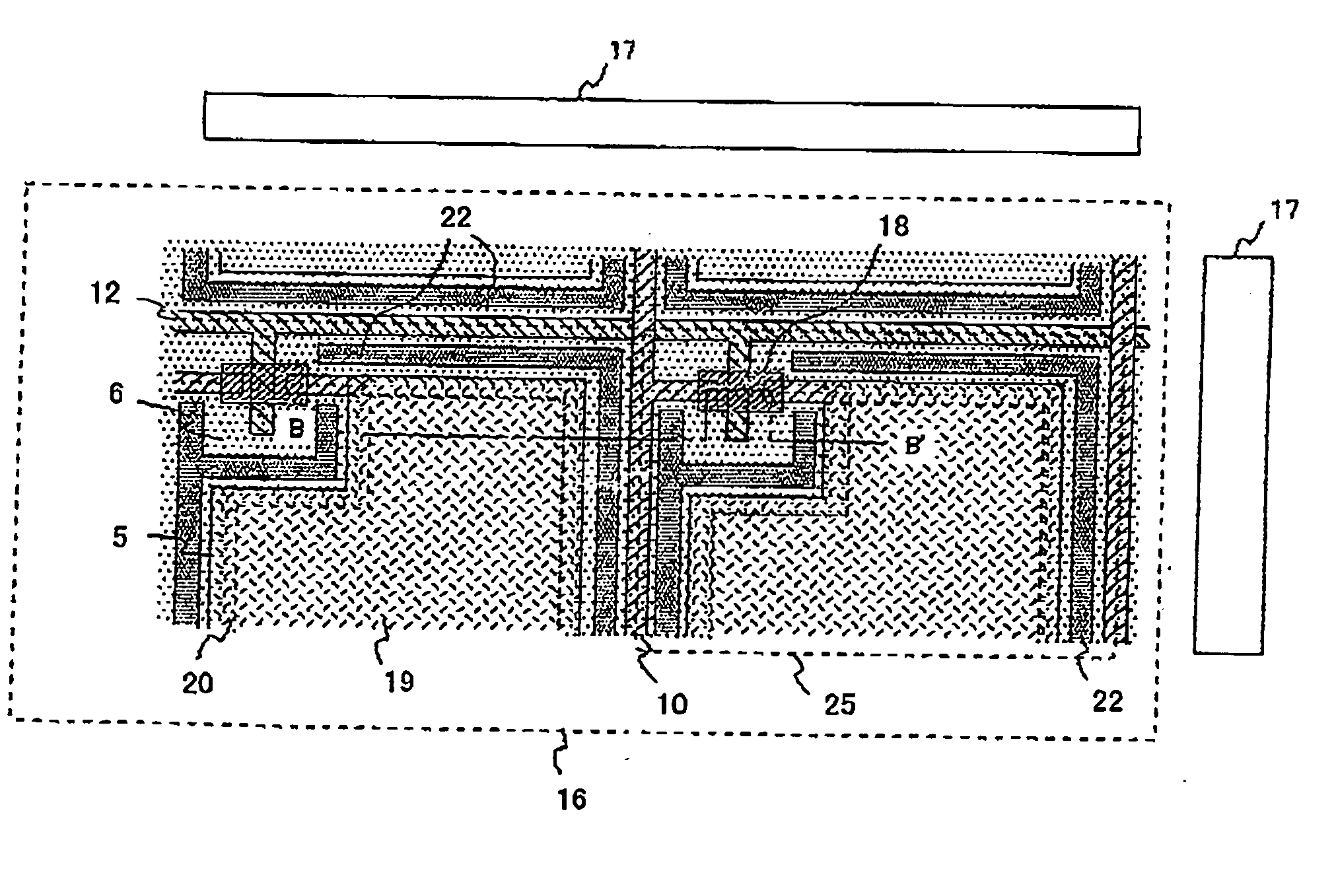
[0050] As shown in FIG. 6, an active matrix organic EL display apparatus includes a plurality of gate lines 12 and data lines 10 extending and crossed in orthogonal direction with each other, and pixel driving TFTs 18 are formed on each of the intersecting points. While one pixel driving TFT 18 is shown in FIG. 6, a plurality of the pixel driving TFTs may be used depending on the drive system. The drain terminal, the source terminal and the gate terminal of the pixel driving TFT 18 are connected to the data line 10, a cathode 5 and the gate line 12, respectively.

[0051] The planerizing layer 6 flattens irregularities generated due to the difference of the heights of the respective elements such as the gate line 12, the data line 10, the pixel driving TFT 18 and the cathode 5, and has an aperture area to expose the top surface of the cathode 5. An EL organic layer 7 and an anode 8 are stacked on the planerizing layer 6 to form an EL element 19 inside the border 20 with the planerizin...

second embodiment

[0066] The present Embodiment is an improvement of the first Embodiment, and the description of the same components as those of the first Embodiment will be omitted by attaching the same numerals thereto.

[0067] As shown in FIGS. 8 and 9, different from the first Embodiment, a light blocking structure 22a is formed around the EL element 19 to separate the pixel driving TFT 18 from the EL element 19, and another light blocking structure 22b is formed around the display region 16 to separate the display region 16 from the peripheral circuit regions 17.

[0068] The light traveling inside the second interlayer 23 emitted from the EL element 19 is reflected partly at the boundary of the light blocking structure 22 and is absorbed partly by the material thereof before reaching the pixel driving TFT 18 so that the intensity of the light traveling inside the second interlayer 23 can be reduced, thereby decreasing the photo leakage current.

[0069] Since the light blocking structure 22b is dis...


PUM


Abstract

A luminescence display apparatus including a light blocking structure having a function of reflecting light propagating through the dielectric layer and/or of attenuating light propagating through the dielectric layer, that surrounds a EL element for separating a pixel driving TFT from the EL element. Self-emitted light or external light be attenuated before reaching the TFT by using the light blocking structure to reduce the photo leakage of the TFT to provide the active matrix organic EL display apparatus having the less defects and the excellent gradation controllability.

Description

TECHNICAL FIELD [0001] The present invention relates to a luminescence display apparatus, and more specifically, to an active matrix organic electro-luminescence (EL) display apparatus including an organic EL section and a driving circuit including an array of thin film transistors (TFTs). The present invention also relates to and a method of fabricating the same. BACKGROUND ART [0002] An organic EL device is a self luminescent device which utilizes the principle that a fluorescent material emits light by using the energy obtained by combination between positive holes injected from a cathode and electrons injected from an anode upon applying an electric field thereon. In these days, the organic EL device attracts attention as a display apparatus in place of CRT and LCD because of a wider viewing angle and an excellent response characteristic. Among the organic EL devices, an active matrix organic EL device attracts special attention in which organic EL devices arranged in matrix are...

Claims


Application Information

Patent Timeline
Patent Type & Authority Applications(United States)
IPC IPC(8): G09F9/30H05B33/10H01J1/62H01L27/32H01L29/786H01L51/50H05B33/14
CPCH01L27/3272H10K59/124H10K59/126H10K50/856
Inventor IGA, DAISUKE
Owner NEC CORP
Why Eureka
Try Eureka