Method for heat treatment of silicon wafer and silicon wafer

a heat treatment method and silicon wafer technology, applied in the direction of silicon compounds, instruments, scanning probe techniques, etc., can solve the problems of degradation of electric characteristics, method does not afford sufficient improvement of electric characteristics, and heat treatment of the aforementioned prior art does not sufficiently improve cop

Inactive Publication Date: 2001-06-12
SHIN-ETSU HANDOTAI CO LTD
View PDF8 Cites 41 Cited by
  • Summary
  • Abstract
  • Description
  • Claims
  • Application Information

AI Technical Summary

Problems solved by technology

These defects are called COP (crystal originated particle), and may be a cause of the degradation of electric characteristics.
Further, the experiments conducted by the inventors of the present invention revealed that the heat treatment of the aforementioned prior art did not sufficiently improve COP, though it improved the oxide dielectric breakdown voltage to some extent.
Therefore, the method did not afford sufficient improvements of electric characteristics except for the oxide dielectric breakdown voltage.
Further, even when the heat treatment was performed at 1100.degree. C., the reduction of COPs was still insufficient like the above case.
That is, it was found that sufficient improvement of COP could not be obtained by the conditions of the heat treatment according to the p

Method used


Image

  • Method for heat treatment of silicon wafer and silicon wafer
  • Method for heat treatment of silicon wafer and silicon wafer
  • Method for heat treatment of silicon wafer and silicon wafer

Examples


Embodiment Construction

The present invention and embodiments thereof will be explained more in detail hereinafter.

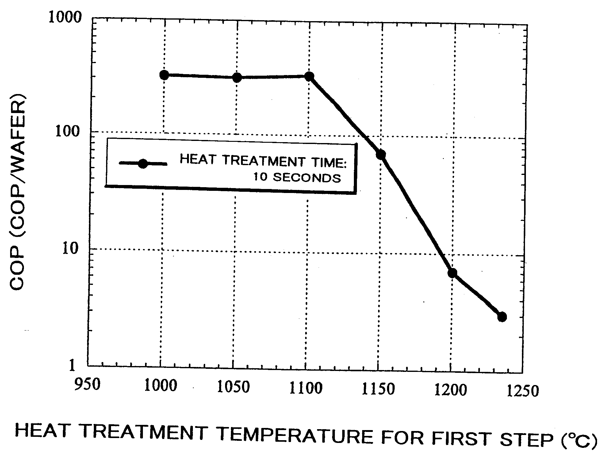
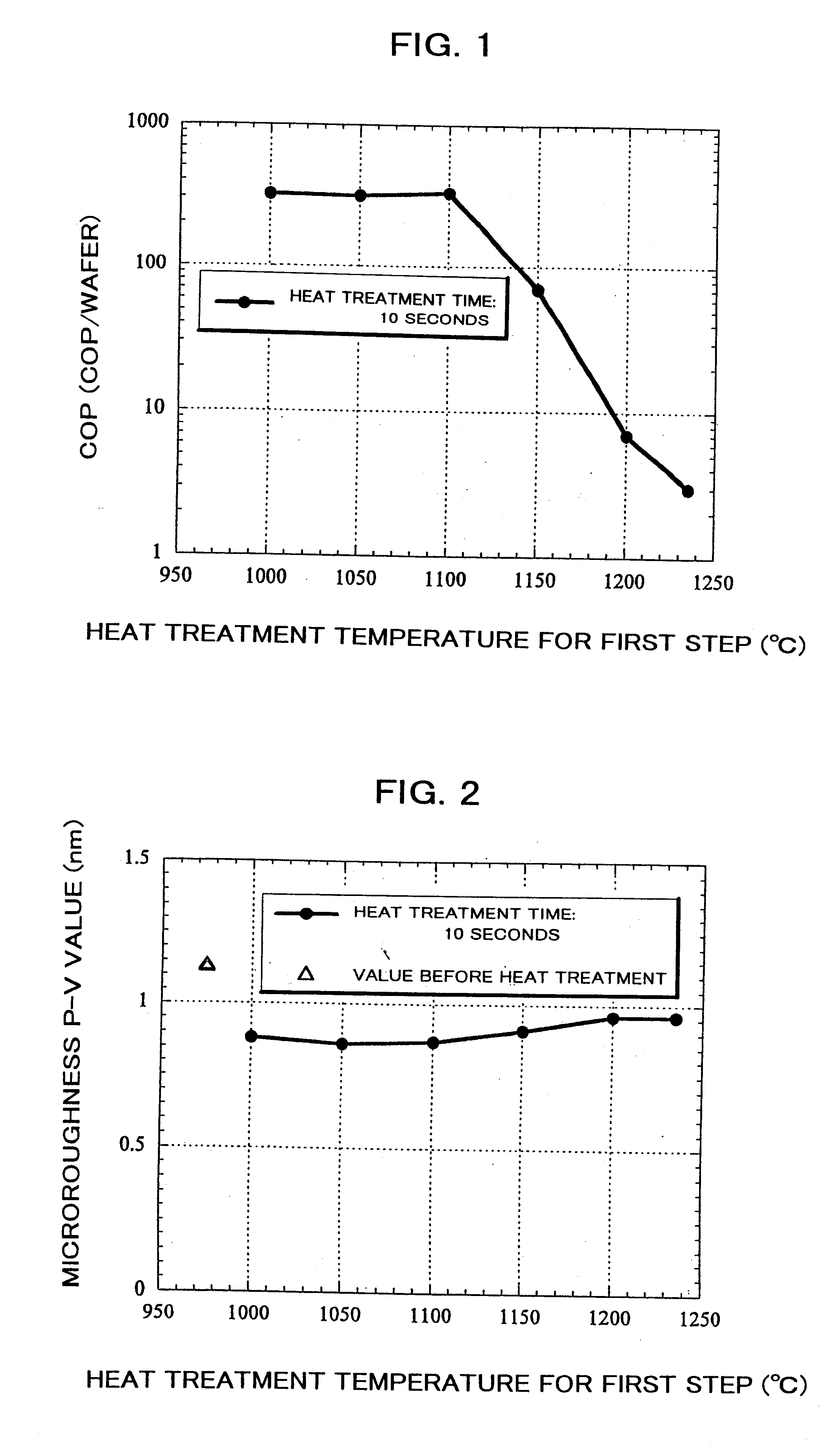
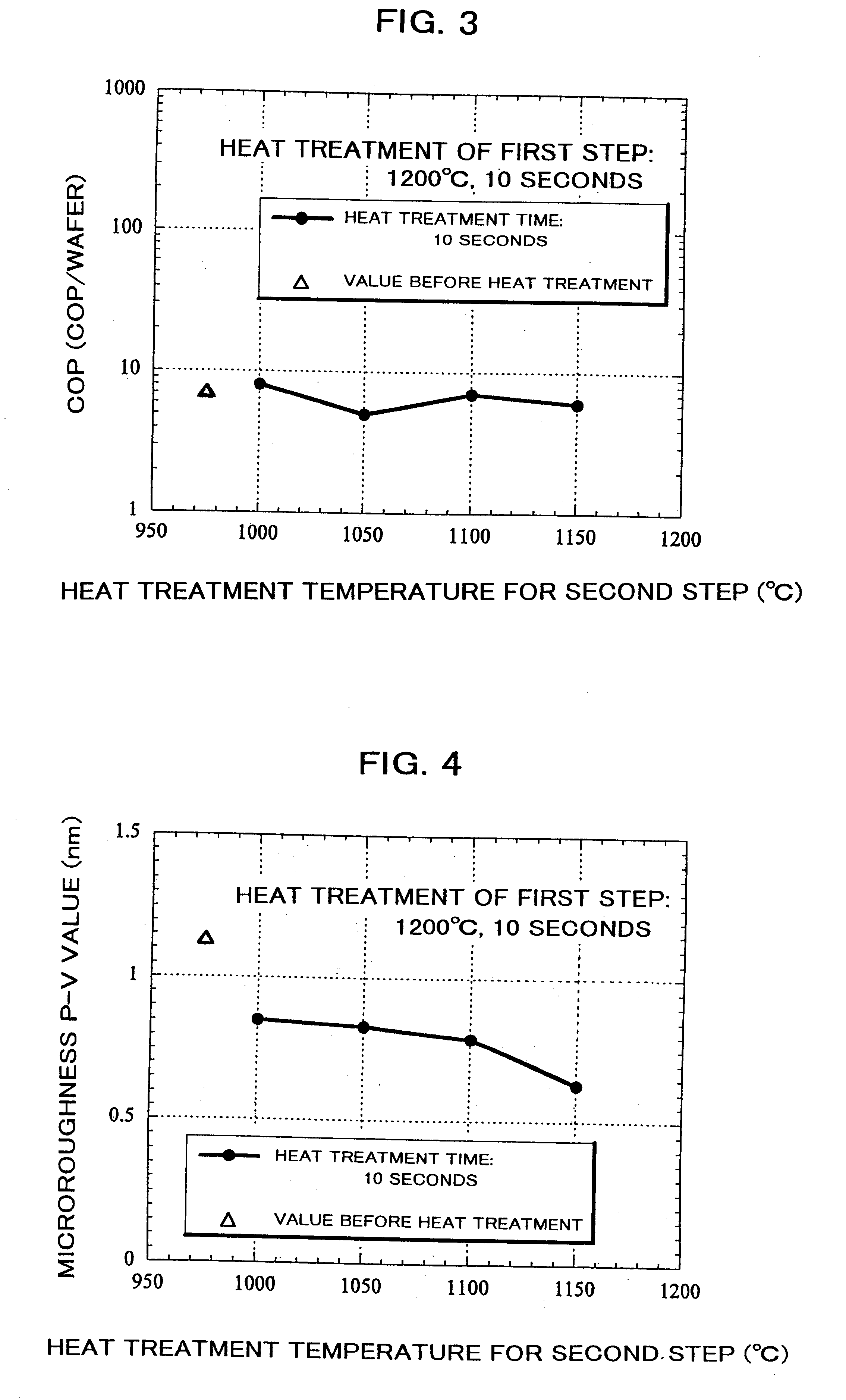
The inventors of the present invention investigated conditions for heat treatment which can reduce the density of COPs present on silicon wafer surface to improve the oxide dielectric breakdown voltage, and decrease microroughness and haze to realize improvements of electric characteristics such as improvement of carrier mobility through various experiments. As a result, they found that, if the heat treatment under the reducing atmosphere containing hydrogen gas is performed by a plurality of steps each of which is performed with a differently defined heat treatment condition, silicon wafers with low COP density and small microroughness and haze can be obtained. Further, they investigated various conditions for the aforementioned characteristics of the present invention, and thus completed the present invention.

First, in order to establish suitable heat treatment conditions for the plurality o...


PUM


Abstract

There is disclosed a method for heat treatment of a silicon wafer performed in a reducing atmosphere containing hydrogen by utilizing a rapid thermal annealer, wherein the heat treatment comprises a plurality of steps each of which is performed with a differently defined heat treatment condition. In this method, the heat treatment comprising a plurality of steps may be continuously performed without taking out the wafer from an RTA apparatus. The method of the present invention can, in particular, reduce COP density of the silicon wafer surface, reduce its microroughness and haze, and thus improve electric characteristics such as oxide dielectric breakdown voltage and mobility of carriers.

Description

1. Field of the InventionThe present invention relates to a method for heat treatment of a silicon wafer, and more particularly, it relates to a method for heat treatment of a silicon wafer that can reduce COP density, and at the same time, decrease microroughness and haze of the silicon wafer surface.2. Description of the Related ArtIn order to improve electric characteristics of silicon wafers such as oxide dielectric breakdown voltage, it is necessary to obtain a wafer surface layer on which devices are fabricated as a defect-free layer. In the surface layer of silicon wafer, there are usually crystal defects having a regular octahedral structure, which are introduced during the crystal growth. These defects are called COP (crystal originated particle), and may be a cause of the degradation of electric characteristics.For improving the oxide dielectric breakdown voltage, it has been reported that it is effective to subject a silicon wafer to hydrogen annealing, i.e., a heat treat...

Claims


Application Information

Patent Timeline
IPC IPC(8): H01L21/02H01L21/322G01Q30/10G01Q60/00H01L21/324
CPCH01L21/3225H01L21/324
Inventor KOBAYASHI, NORIHIROAKIYAMA, SHOJIMIYANO, TOSHIHIKO
Owner SHIN-ETSU HANDOTAI CO LTD
Why Eureka
Try Eureka