
Semiconductor device

a technology of semiconductor devices and conductive bonding materials, applied in the field of semiconductor devices, can solve problems such as defective operation, heat generation of semiconductor devices of this kind, and cracks in second conductive bonding materials, and achieve the effect of preventing a defective operation

Inactive Publication Date: 2005-06-09
DENSO CORP
View PDF7 Cites 26 Cited by
  • Summary
  • Abstract
  • Description
  • Claims
  • Application Information

AI Technical Summary

Benefits of technology

[0013] The present invention, in view of the above problems, devises a semiconductor device with a main electrode on each of the main side and the main reverse side of the semiconductor element having a first metal body on the main reverse side and a second / third metal body on the main side, and also having a heat sensing diode on the main side of the semiconductor element, most of the device covered by a molding material, such as a resin. The inventive structure of the semiconductor device prevents a defective operation of the heat sensing diode caused by a crack in the conductive bonding material between the main side of the semiconductor element and the second metal body.
[0015] Because of the arrangement of the heat sensing diode on the main side of the semiconductor element, a crack on the periphery of the second conductive bonding material does not affect the operation of the heat sensing diode, and thus the structure minimizes the risk of malfunction of the device.

Problems solved by technology

However, the semiconductor device of this kind suffers from heat generation because of the density of implementation and the like.
This situation leads to a possibility of crack in the second conductive bonding material 52 between the semiconductor element 10 and the second metal body 40 in FIG. 4A.
The interrupted heat dissipation path causes heat accumulation around the heat sensing diode 11 resulting in a defective operation.

Method used


Image

  • Semiconductor device
  • Semiconductor device
  • Semiconductor device

Examples


first embodiment

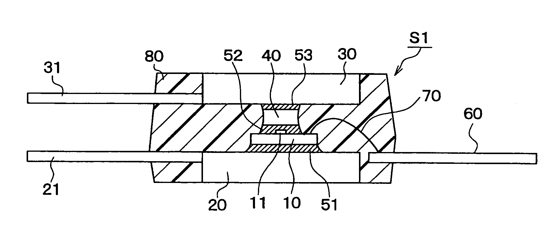
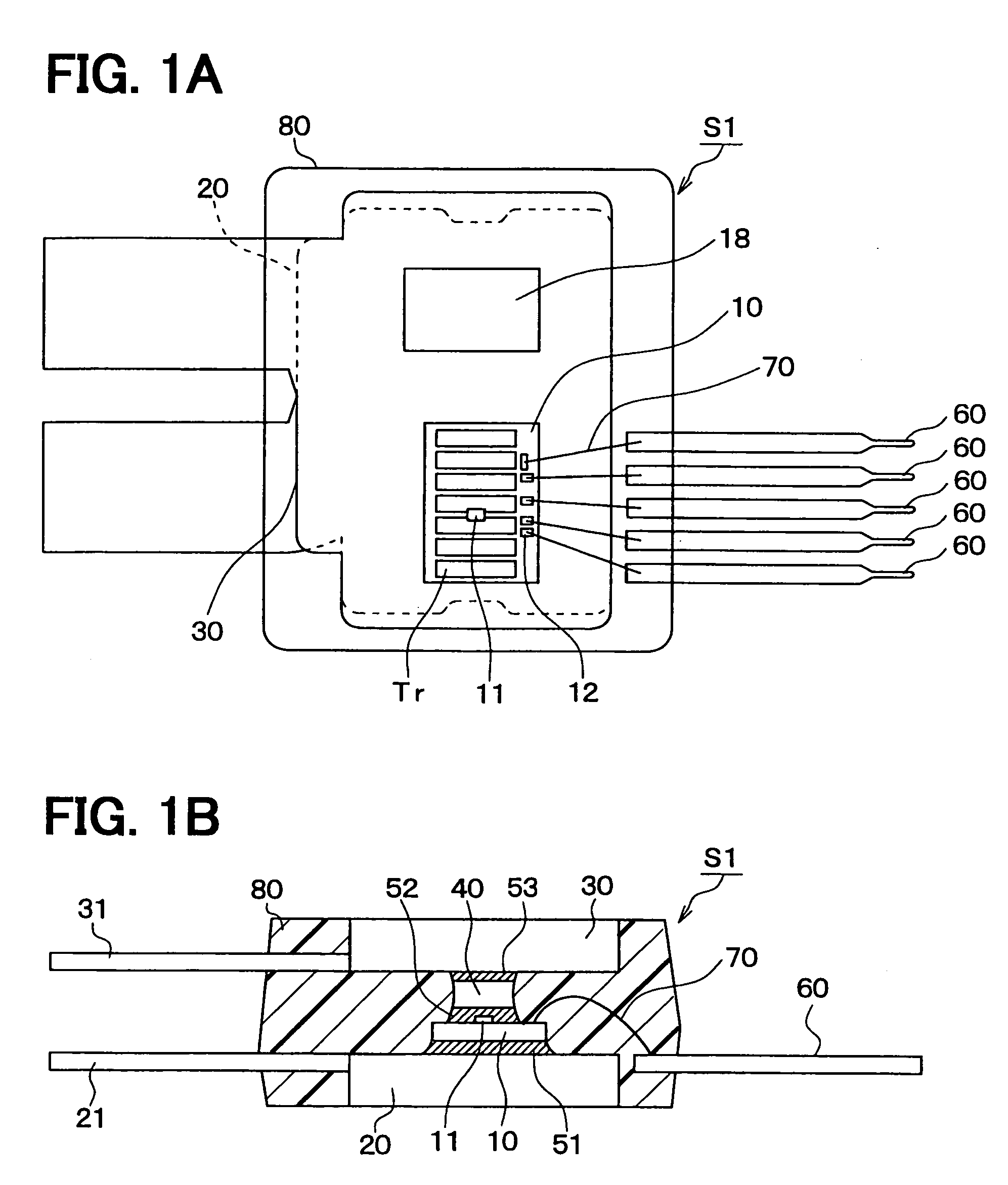
[0027] A semiconductor device S1 in the present embodiment, as shown in FIGS. 1A, 1B, 2A and 2B, comprises a first semiconductor chip 10 as a semiconductor element, a lower heatsink 20 as a first metal body, an upper heatsink 30 as a third metal body, a heatsink block 40 as a second metal body, conductive bonding materials 51, 52, 53 placed between the semiconductor element and the metal bodies, a heat sensing diode 11 disposed on the first semiconductor chip 10, and a resin mold 80.

[0028] In the present embodiment, the first semiconductor chip 10 is sided by a second semiconductor chip 18. In this structure, downsides of the semiconductor chips 10, 18 and an upside of the lower heatsink 20 are bonded by a first conductive bonding material 51. Further, upsides of the semiconductor chips 10, 18 and downsides of the heatsink blocks 40 are bonded by a second conductive bonding material 52. Furthermore, upsides of the heatsink blocks 40 and a downside of an upper heatsink 30 are bonded...

second embodiment

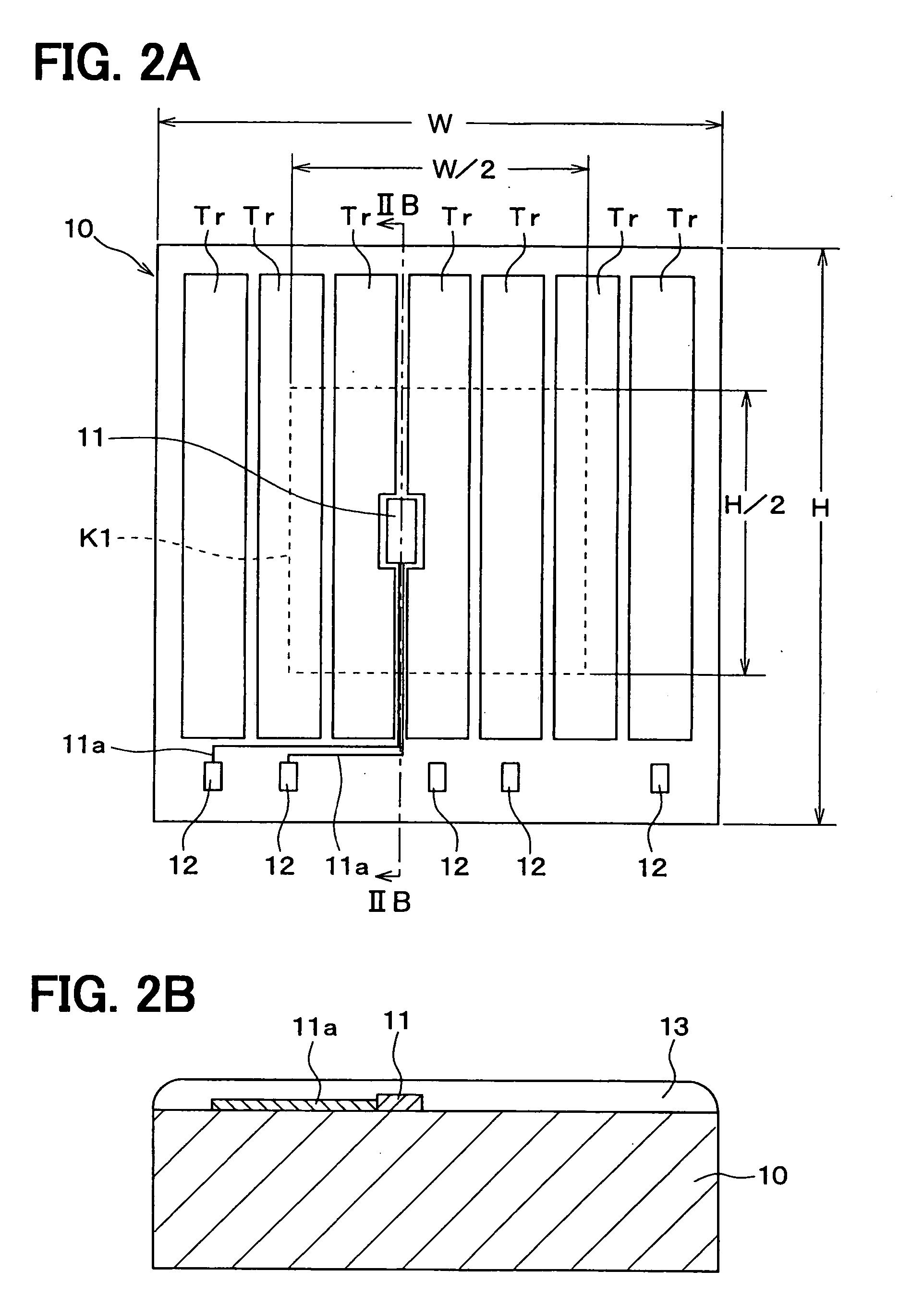
[0084] In this embodiment shown in FIG. 3, the multiple cell blocks Tr are arranged in a row on the main side of the first semiconductor chip 10. The number of the cell block Tr is even (e.g. eight).

[0085] In this case, the heat sensing diode 11 is disposed between the two cell blocks Tr at the center in the row. According to this arrangement, the heat sensing diode 11 can appropriately be disposed at the center of the main side on the first semiconductor chip 10.

[0086] Except for the difference described above, the semiconductor device in this embodiment provides the same operational effect as in the first embodiment.

Other Embodiments

[0087] The semiconductor element used for this invention is not limited to the power semiconductor element such as an IGBT, a thyristor, and the like, but a semiconductor element with a main electrode on a main side and a main reverse side.


PUM


Abstract

In a semiconductor device, risk of malfunction of a heat sensing diode on a main side of a vertical power semiconductor element is minimized by arranging the diode at the center of the element. Because the heat sensing diode is disposed at the center of the main side of the semiconductor element, the diode is protected from breakage and heat accumulation even when an excessive heat causes a crack at the periphery of a conductive bonding material that connects the element and the metal bodies on both sides of the element.

Description

CROSS REFERENCE TO RELATED APPLICATION [0001] This application is based on and incorporates herein by reference Japanese Patent Application No. 2003-405911 filed on Dec. 4, 2003. FIELD OF THE INVENTION [0002] The present invention relates to a semiconductor device that has a semiconductor element with a main electrode on each of its main side and its main reverse side. The semiconductor element has a first metal body on the main reverse side and second and third metal bodies on the main side, and also has a heat sensing diode for detecting temperature on the main side. The semiconductor device has a resin cover molded on it. BACKGROUND OF THE INVENTION [0003] In FIG. 4A and FIG. 4B, a typical semiconductor device of this kind is shown schematically. The semiconductor device shown in FIG. 4A is proposed, for example, in US 2003 / 0022464 (JP-A-2003-110064). [0004] In FIG. 4A, the semiconductor element 10 is, for example, a vertical power element such as an IGBT (Insulated Gate Bipolar ...

Claims


Application Information

Patent Timeline
IPC IPC(8): H01L21/822G01K7/01H01L23/31H01L23/34H01L23/433H01L23/48H01L23/495H01L25/16H01L27/04
CPCG01K7/01H01L23/3107H01L2924/1305H01L2924/1301H01L24/49H01L2924/01033H01L2924/01006H01L24/48H01L2924/13055H01L2924/01082H01L2924/01079H01L2924/01074H01L2924/0105H01L2924/01029H01L2924/01013H01L23/34H01L23/4334H01L23/49568H01L24/33H01L25/165H01L2224/32245H01L2224/48091H01L2224/48247H01L2224/49171H01L2224/73215H01L2224/73265H01L2924/01005H01L2924/00014H01L2924/00H01L2924/3512H01L2924/181H01L2224/05553H01L2224/45124H01L2224/45144H01L24/45H01L2224/2612H01L2924/00012H01L2224/45015H01L2924/207
Inventor HIRANO, NAOHIKOAMANO, SHINJISAKAKIBARA, RIKA
Owner DENSO CORP
Learn More