Piezoelectric device, liquid jetting head, ferroelectric device, electronic device and methods for manufacturing these devices

a technology of liquid jetting head and piezoelectric film, which is applied in the direction of piezoelectric/electrostrictive/magnetostrictive devices, printing, generators/motors, etc., can solve the problems of difficult production of piezoelectric film or ferroelectric film with in-plane orientation, and achieve the effect of efficient manufacturing

Inactive Publication Date: 2005-06-09
SEIKO EPSON CORP
View PDF1 Cites 40 Cited by
  • Summary
  • Abstract
  • Description
  • Claims
  • Application Information

AI Technical Summary

Benefits of technology

[0008] It is an object of the present invention to provide a method for the efficient manufacture of piezoelectric devices or ferroelectric devices comprising piezoelectric films or ferroelectric films which have an in-plane orientation.

Problems solved by technology

However, the efficient production of piezoelectric films or ferroelectric films with an in-plane orientation has been difficult.

Method used


Image

  • Piezoelectric device, liquid jetting head, ferroelectric device, electronic device and methods for manufacturing these devices
  • Piezoelectric device, liquid jetting head, ferroelectric device, electronic device and methods for manufacturing these devices
  • Piezoelectric device, liquid jetting head, ferroelectric device, electronic device and methods for manufacturing these devices

Examples


first embodiment

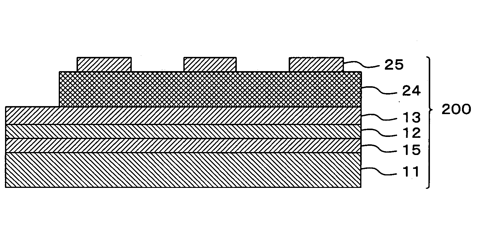
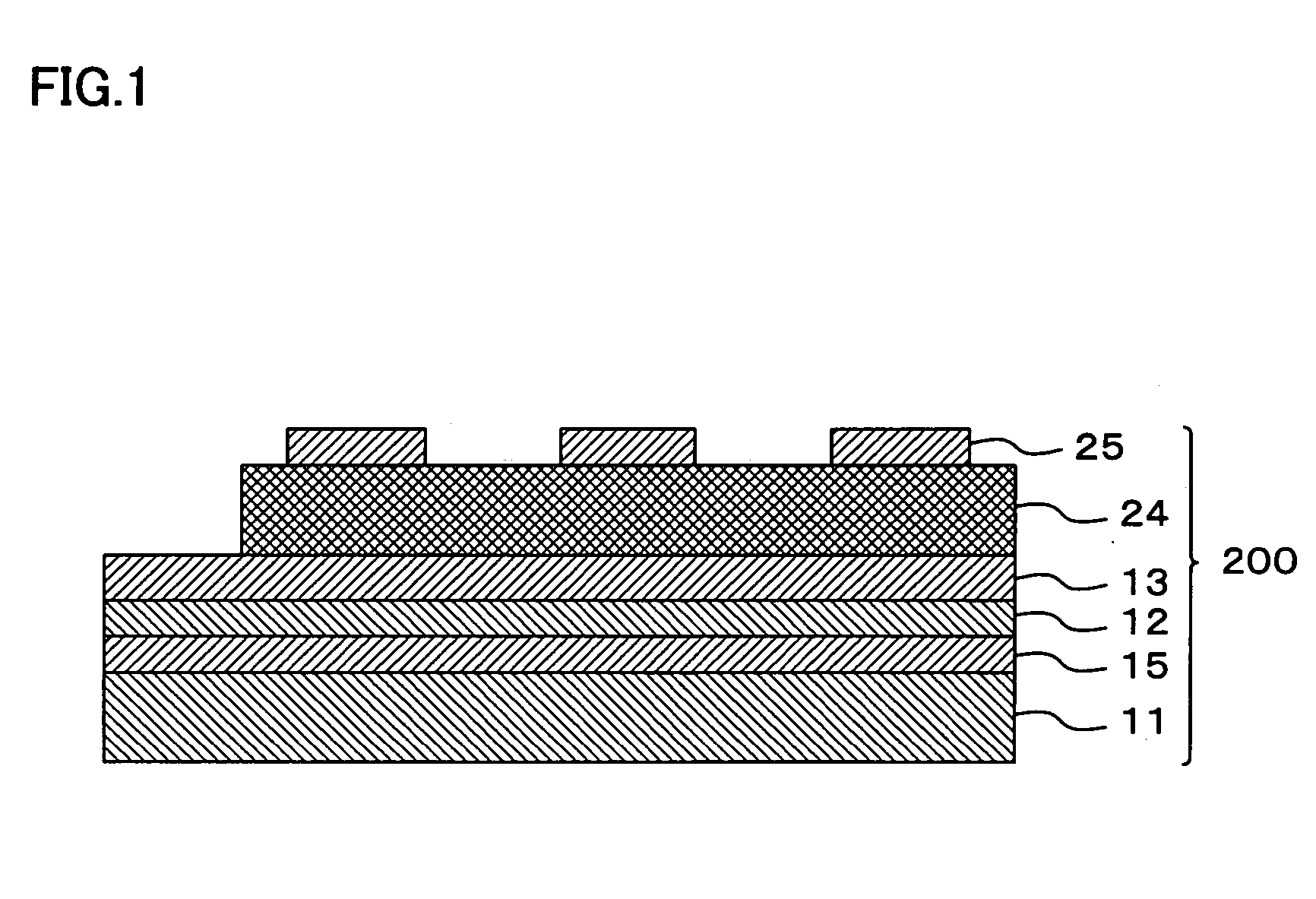
[0083]FIG. 1 is a sectional view of a capacitor constituting a ferroelectric device of the present invention. First, a capacitor 200 which is the ferroelectric device will be described.

[0084] The capacitor 200 of the first embodiment comprises a substrate 11, an amorphous insulating layer 15 which is the first layer of an intermediate film formed on the substrate 11, a buffer layer 12 which is the second layer of this intermediate film, and which is formed on the insulating layer 15, a bottom electrode 13 which is formed on top of this buffer layer 12, a ferroelectric film 24 which is formed in a specified region on top of this bottom electrode 13, and a top electrode 25 which is formed on top of the ferroelectric film 24. In particular, in the present embodiment, the ferroelectric film 24 is formed by an ion beam assist method.

1-1. Substrate

[0085] The substrate 11 has the function of supporting the bottom electrode 13 and the like, and is constructed from a flat-plate-form membe...

second embodiment

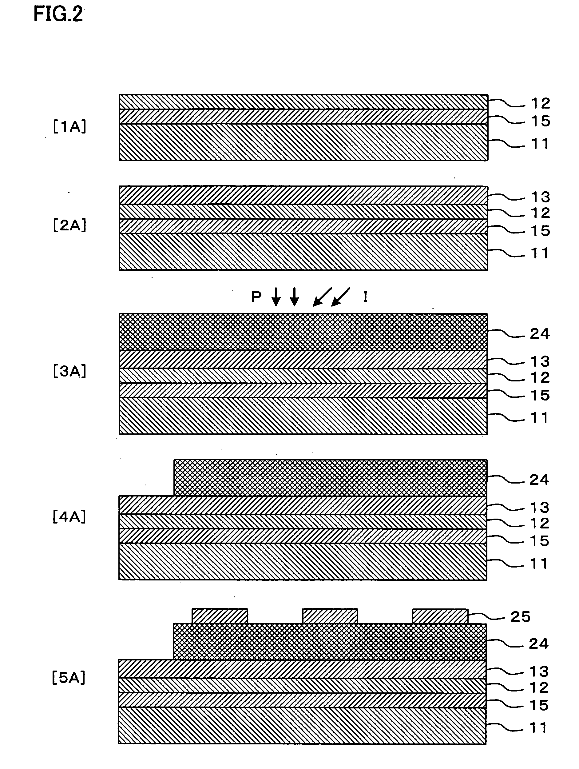
[0153] Next, a manufacturing method for such a capacitor 200 [of the present invention] will be described with reference to FIG. 3. This capacitor 200 can be manufactured by the following steps.

[1B] Buffer Layer Formation Step

[0154] This step can be performed in the same manner as the abovementioned step [1A].

[2B] Bottom Electrode Formation Step

[0155] This step can be performed in the same manner as the abovementioned step [2A].

[3B′] Ferroelectric Precursor Film Formation Step

[0156] A ferroelectric film 24 is formed following the formation of the bottom electrode 13. For example, this can be accomplished as follows. Furthermore, it is desirable to cause the crystal growth of the ferroelectric film 24 to proceed from the bottom electrode side with Ti crystals as nuclei by forming a Ti layer (not shown in the figures) to a thickness of 3 to 7 nm, preferably 4 to 6 nm, by a sputtering method or the like prior to the formation of the ferroelectric film 24.

[0157] First, a ferro...

third embodiment

[0192] Next, a manufacturing method for such a capacitor 200 [of the present invention] will be described with reference to FIG. 4.

[1C] Buffer Layer Formation Step

[0193] This step can be performed in the same manner as the abovementioned step [1A].

[2C] Bottom Electrode Formation Step

[0194] Next, a bottom electrode 13 is formed on top of the insulating layer 15 or on top of the buffer layer 12 of the substrate 11. For example, this bottom electrode 13 can be formed as follows:

[0195] First, the substrate 11 on which an insulating film 15 (or if necessary a buffer layer 12) has been formed is mounted in a substrate holder and placed inside a vacuum apparatus. A first target containing the constituent elements of the bottom electrode 13 as described above (bottom electrode target) is disposed facing the insulating layer 15 of the substrate 11 in a position that is separated from the substrate 11 by a specified distance inside the vacuum apparatus. Furthermore, a target with a com...


PUM


Abstract

An intermediate film (15, 12, 53) is formed on a substrate (11, 52), a bottom electrode (13, 542) is formed on top of this intermediate film, a ferroelectric film (24) or piezoelectric film (543) is formed on top of this bottom electrode by an ion beam assist method, and a top electrode (25, 541) is formed on top of this ferroelectric film or piezoelectric film. The ferroelectric film or piezoelectric film is formed by PZT, BST or a relaxer material. As a result of the use of an ion beam assist method in the formation of any one of the intermediate film, bottom electrode, ferroelectric film or piezoelectric film, a piezoelectric device or ferroelectric device which has a piezoelectric film or ferroelectric film with an in-plane orientation can be manufactured with good efficiency.

Description

BACKGROUND OF THE INVENTION [0001] 1. Field of the Invention [0002] The present invention relates to a piezoelectric device or ferroelectric device comprising a piezoelectric film or ferroelectric film and a pair of electrodes between which this film is sandwiched, and a liquid jetting head and electronic device equipped with such devices, and more particularly relates to a piezoelectric device or the like comprising a piezoelectric film or ferroelectric film which has superior orientation properties. [0003] 2. Description of the Related Art [0004] Compound oxides which have a perovskite type crystal structure and which can be expressed by the chemical formula ABO3 are known as piezoelectric films or ferroelectric films used in piezoelectric devices or ferroelectric devices. For example, lead zirconate titanate (PZT) which uses lead (Pb) as A and a mixture of zirconium (Zr) and titanium (Ti) as B is known. [0005] In order to improve the characteristics of such piezoelectric films or...

Claims


Application Information

Patent Timeline
Patent Type & Authority Applications(United States)
IPC IPC(8): B41J2/16H01L21/316H01L41/047H01L41/09H01L41/22
CPCB41J2/161B41J2/1623B41J2/1628B41J2/1629B41J2/1634H01L41/0973B41J2/1643B41J2/1645B41J2/1646H01L21/31691H01L41/316B41J2/1642H01L21/02197H10N30/2047H10N30/076H10N30/80
Inventor HIGUCHI, TAKAMITSUIWASHITA, SETSUYAMIYAZAWA, HIROMUSUMI, KOJIMURAI, MASAMIITO, MAKIXIN-SHAN, LI
Owner SEIKO EPSON CORP
Why Eureka
Try Eureka