Data element size control within parallel lanes of processing

US20050125631A1Inactive Publication Date: 2005-06-09ARM LTD
61 Cites 42 Cited by

Patent Information

Authority / Receiving Office
US · United States
Current Assignee / Owner
Publication Date
2005-06-09
Estimated Expiration
Not applicable · inactive patent

Smart Images

  • Figure 1
    Figure 1
  • Figure 2
    Figure 2
  • Figure 3
    Figure 3
Patent Text Reader

Abstract

Within a SIMD processor 2 data processing instructions are provided which specify parallel lanes of processing to be performed upon respective data elements. The data elements are permitted to vary in size whilst the number of processing lanes remain constant. Thus, the destination register size for a multiplication may be double the source register size.
Need to check novelty before this filing date? Find Prior Art

Description

BACKGROUND OF THE INVENTION

[0001] 1. Field of the Invention

[0002] This invention relates to the field of data processing systems. More particularly, this invention relates to data processing systems in which data processing instructions perform a data processing operation in a number of parallel lanes of processing on respective data elements from within a source register so as to generate respective data elements within a destination register.

[0003] 2. Description of the Prior Art

[0004] It is known to provide SIMD (single instruction multiple data) processors in which a data processing operation upon a specified register results in parallel operations upon multiple data elements stored within that register, each of those elements being treated as part of a lane of processing. As an example, a register may contain multiple data elements each representing a component value of a pixel. It may be desired to scale those component values by certain amounts and this can be achieved us...

Examples

Embodiment Construction

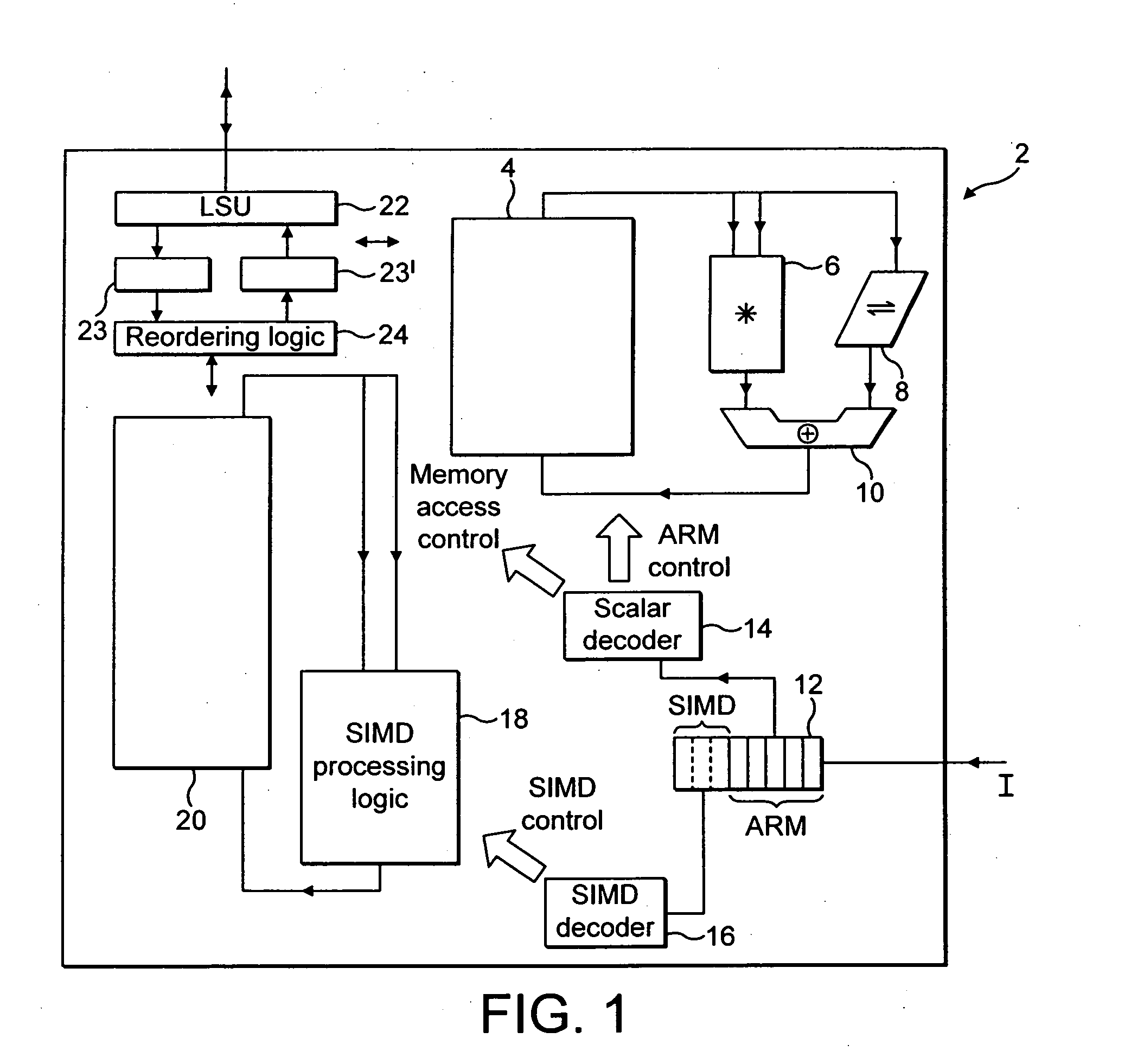
[0082]FIG. 1 schematically illustrates a data processing system (integrated circuit) 2 incorporating both a scalar data processing functionality and a SIMD data processing functionality. The scalar data processing portion can be considered to be a standard ARM processor core incorporating a scalar register data store 4, a multiplier 6, a shifter 8, an adder 10, an instruction pipeline 12 and a scalar decoder 14 as well as many other circuit elements which have not, for the sake of clarity, been illustrated. In operation, such a scalar processor core stores fixed length 32-bit data values within the scalar register data store 4 and manipulates these using the multiplier 6, shifter 8 and adder 10 under control of data processing instructions passed along the instruction pipeline 12 and supplied to the scalar decoder 14. The scalar decoder 14 produces control signals which control the operation of the scalar processing elements in a conventional way.

[0083] As illustrated in FIG. 1 the...