Method and system for defect evaluation using quiescent power plane current (IDDQ) voltage linearity

a power plane current and defect evaluation technology, applied in the field of integrated circuit test systems, can solve problems such as general inacceptability of defects, and achieve the effect of reducing the number of defects

Inactive Publication Date: 2005-06-09
IBM CORP
View PDF6 Cites 9 Cited by
  • Summary
  • Abstract
  • Description
  • Claims
  • Application Information

AI Technical Summary

Benefits of technology

[0010] The objective of providing an improved IDDQ testing algorithm that distinguishes between shorts that will cause functional failures and shorts that will not is provided in a method and system for performing voltage-dependent IDDQ testing that detects an onset of non-linear behavior of IDDQ versus VDD in order to determine the relative magnitude of the shorting resistance and the driving resistance.

Problems solved by technology

If the slope changes over the entire range of voltages, a defect is present that is generally unacceptable.

Method used


Image

  • Method and system for defect evaluation using quiescent power plane current (IDDQ) voltage linearity
  • Method and system for defect evaluation using quiescent power plane current (IDDQ) voltage linearity
  • Method and system for defect evaluation using quiescent power plane current (IDDQ) voltage linearity

Examples


Embodiment Construction

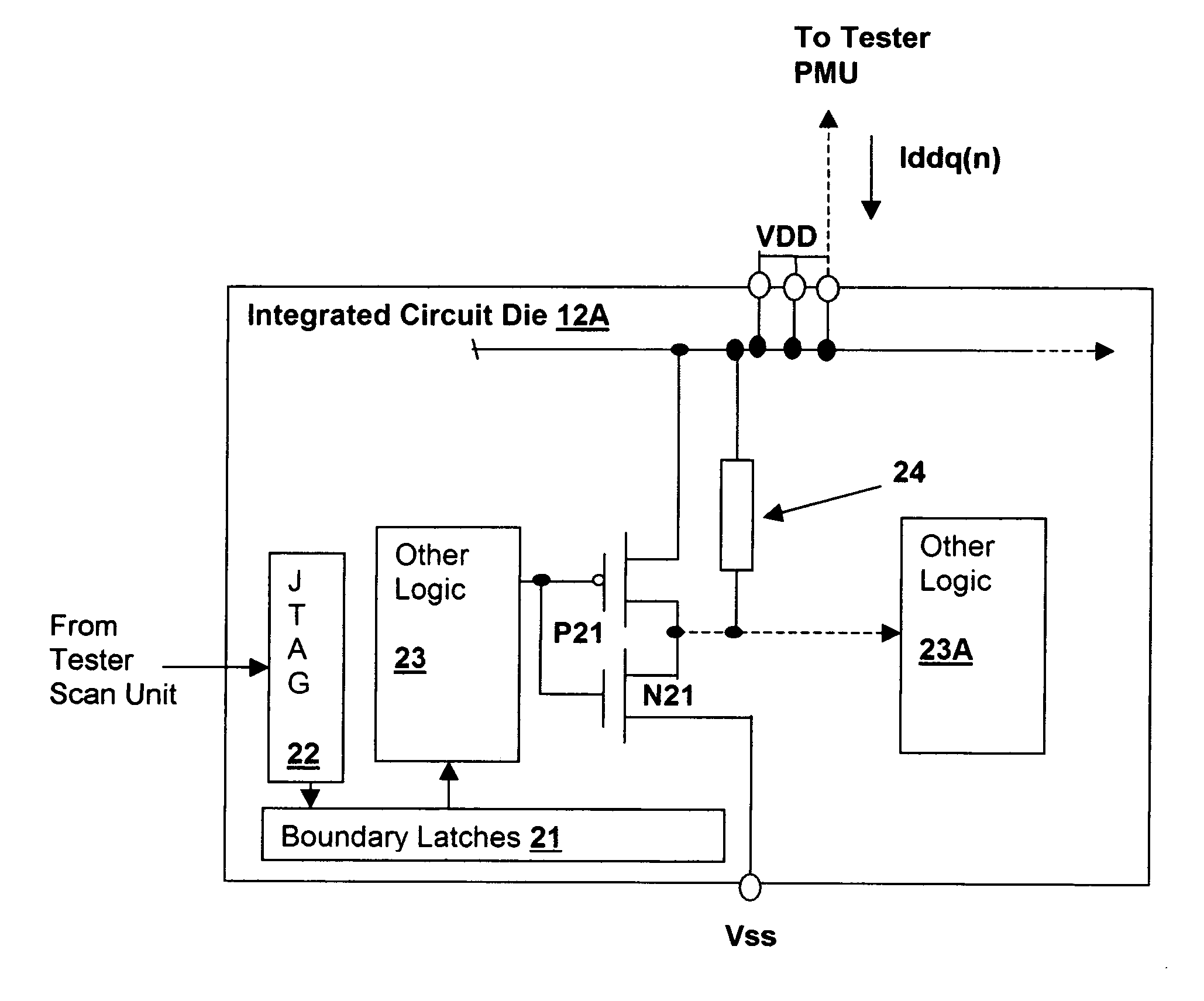
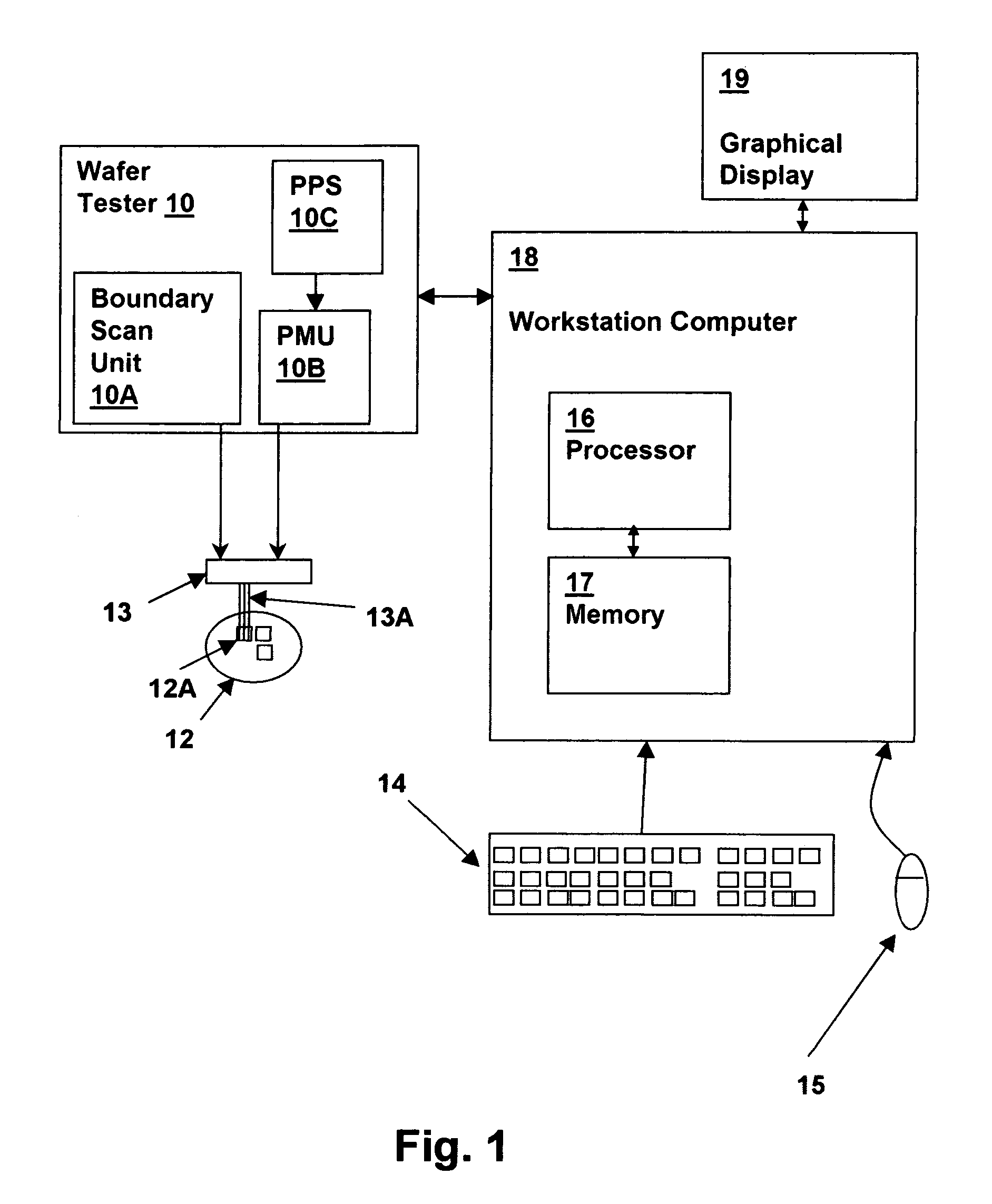
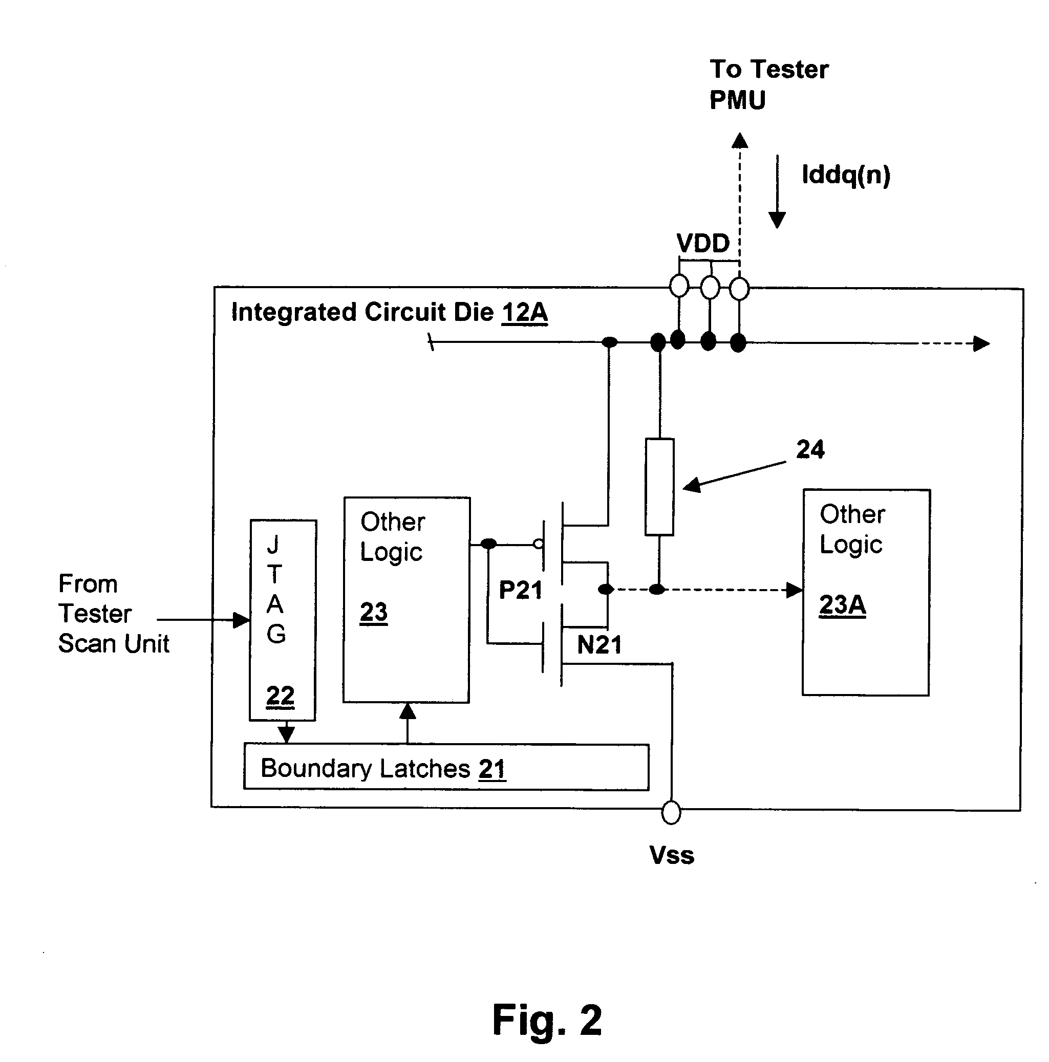
[0020] Referring to the figures, and particularly to FIG. 1, a VLSI wafer test system, in which methods according to an embodiment of the present invention are performed, is depicted. A wafer tester 10 includes a boundary scan unit 10A for providing stimulus to a die 12A on a wafer under test 12, via a probe head 13 having electrical test connections 13A to die 12A. Wafer tester 10 also includes a parametric measurement unit (PMU) 10B, also coupled to die 12A via probe head 13 via electrical test connections 13A that can measure analog parameters such as the power plane current (IDDQ) as measured in accordance with the methods of the present invention. Wafer tester 10 further includes a programmable power supply (PPS) 10C that provides for programming multiple differing power plane voltages (VDDS) and is coupled to PMU 10B so that the power supply current supplied by PPS 10C can be measured by PMU 10B. IDDQ measurements are performed over a series of test vectors stimulated by bound...


PUM


Abstract

A method and system for defect evaluation using IDDQ voltage linearity provides improved IDDQ testing for determining whether manufacturing defects in a VLSI device are likely to cause functional faults. IDDQ data is collected at multiple power plane voltages (VDDs) for a test vector at which a fault is activated. The IDDQ vs. VDD is then examined and a range of VDDs over which the characteristic IDDQs are non-linear with respect to VDD is determined. Peaks in the first derivative of the IDDQ vs. VDD curve indicate a particular VDD at which the onset of non-linearity in the IDDQ occurs. The VDD point below which the curve is non-linear indicates the relative resistance of a fault with respect to the driving point resistance of the node at which the fault is located. The relative resistance is directly determinative of additional circuit delay cause by the fault and/or whether the fault will cause a logic level transmission failure. Therefore, the range of VDDs for which the IDDQ curve is linear provides a pass/fail indication that can be used to reject devices in manufacturing test.

Description

BACKGROUND OF THE INVENTION [0001] 1. Field of the Invention [0002] The present invention generally relates to integrated circuit test systems, and more particularly to a computer program that analyzes voltage dependency of integrated circuit power supply pin quiescent current measurements. [0003] 2. Description of Related Art [0004] Manufacturing tests and design verification tests are necessary for ensuring functionality and reliability of large-scale digital integrated circuits such as Very Large Scale Integration (VLSI) circuits. Millions of transistors and logic gates are often combined on a single die and the performance of the die is verified both in the design phase and the manufacturing phase of a VLSI product cycle. [0005] Power supply current for individual gates or blocks within such a VLSI circuit combines to generate the power requirements for the overall die, and will typically combine in sub-groups to several power and ground pins that are typically also connected wi...

Claims


Application Information

Patent Timeline
Patent Type & Authority Applications(United States)
IPC IPC(8): G01R31/30G06F11/00
CPCG01R31/3008
Inventor GATTIKER, ANNE ELIZABETHNIGH, PHILLIP J.
Owner IBM CORP
Why Eureka
Try Eureka