Electrostatic discharge protection with input impedance

a technology of input impedance and electrostatic discharge, which is applied in the direction of emergency protective arrangements for limiting excess voltage/current, electrical equipment, and semiconductor devices, etc., can solve the problems of many of the integrated circuit's external connections floating and being exposed to damage, and the voltage and current of electrostatic discharge can be a major source of damage for integrated circuits

Inactive Publication Date: 2005-06-16
MICRON TECH INC
View PDF11 Cites 8 Cited by
  • Summary
  • Abstract
  • Description
  • Claims
  • Application Information

AI Technical Summary

Problems solved by technology

Electrostatic discharge (ESD) voltage and current can be a major source of damage for integrated circuits.
ESD can be a problem with an integrated circuit that is not in operation or coupled to a circuit.
At these times, many of the integrated circuit's external connections are floating and exposed to damage.
The potential for ESD damage has become even more of a predominant issue with the decreasing device sizes, spacing, and operating voltages of modern components, all of which has the effect of increasing the likelihood of an ESD event causing damage.
ESD protection circuitry, however, while necessary for ESD event survival, can interfere with signal transmission speed and increase capacitive loading when the integrated circuit is operation.
However, these heavier duty components typically also have a higher input drive requirements and corresponding signal propagation delays that can become unacceptable to the design specifications of the integrated circuit.
Unfortunately, this technique can cause a significant signal propagation delay issue by adding a higher RC time constant when the ESD input resistance is combined with the capacitive load of the input circuit and interconnect line.
This leads to issues of varying RC time delay on different input lines, a significant issue in high speed and synchronous design.

Method used


Image

  • Electrostatic discharge protection with input impedance
  • Electrostatic discharge protection with input impedance
  • Electrostatic discharge protection with input impedance

Examples


Embodiment Construction

[0021] In the following detailed description of the preferred embodiments, reference is made to the accompanying drawings that form a part hereof, and in which is shown by way of illustration specific preferred embodiments in which the inventions may be practiced. These embodiments are described in sufficient detail to enable those skilled in the art to practice the invention, and it is to be understood that other embodiments may be utilized and that logical, mechanical and electrical changes may be made without departing from the spirit and scope of the present invention. The following detailed description is, therefore, not to be taken in a limiting sense, and the scope of the present invention is defined only by the claims.

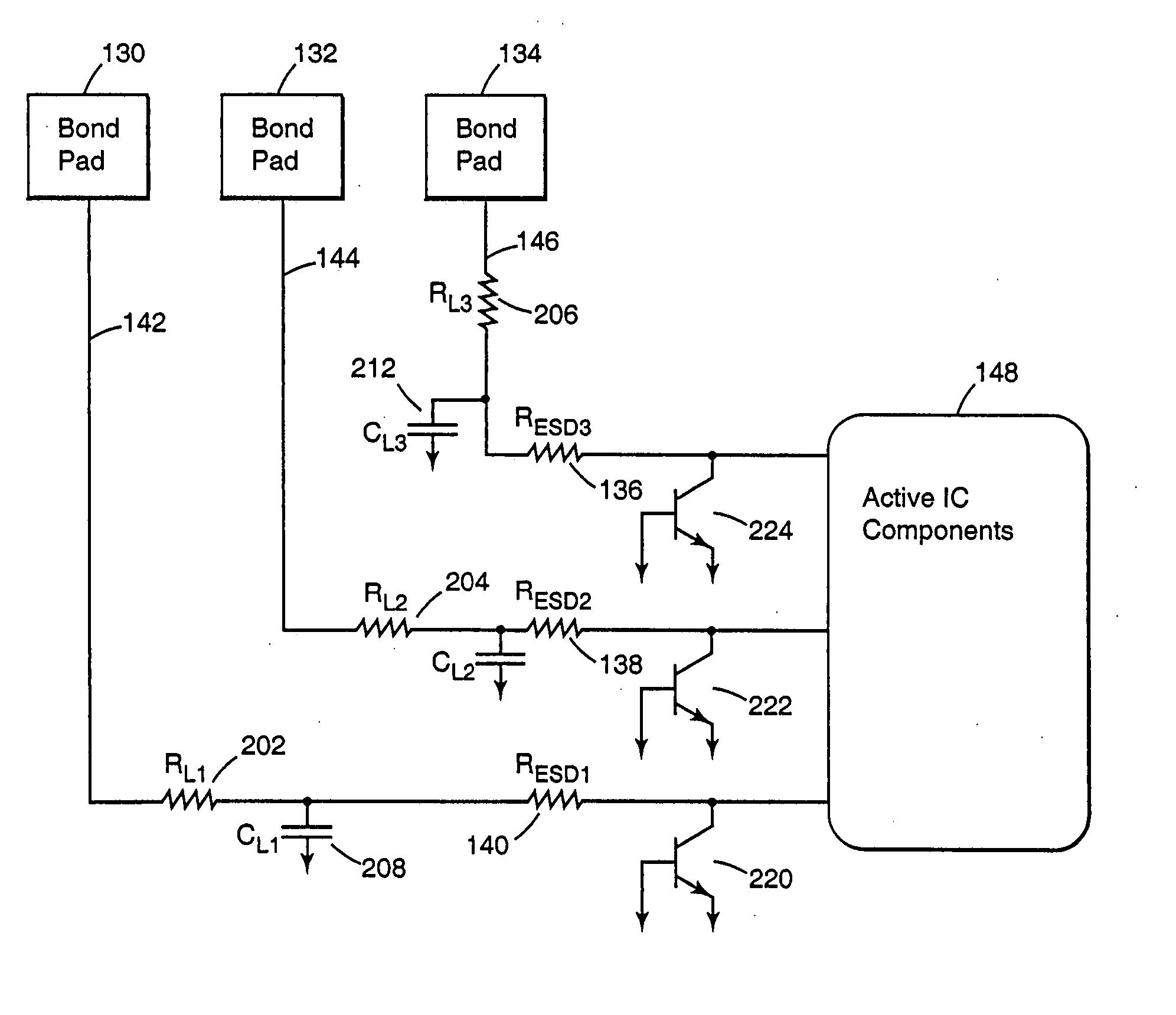
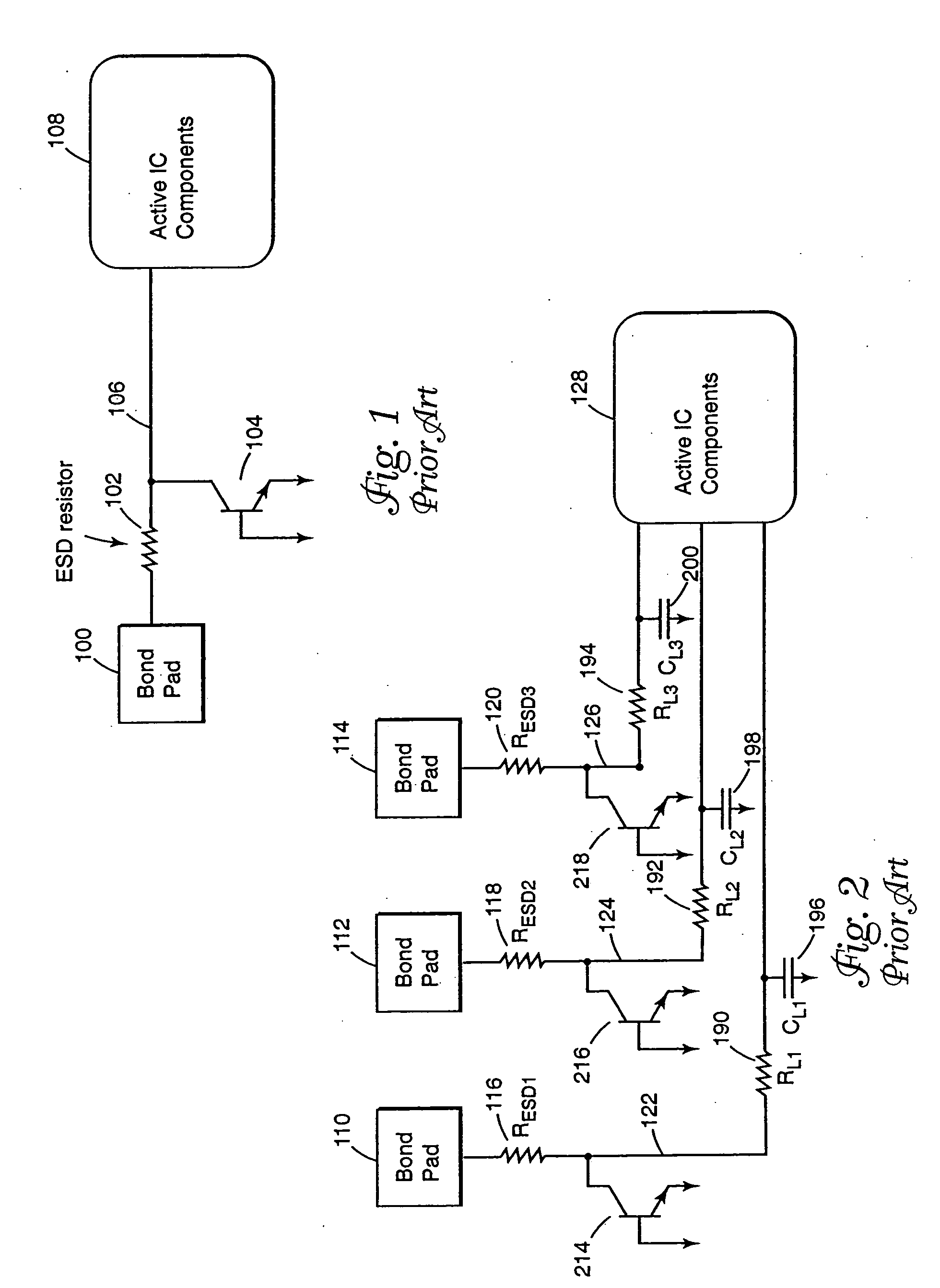
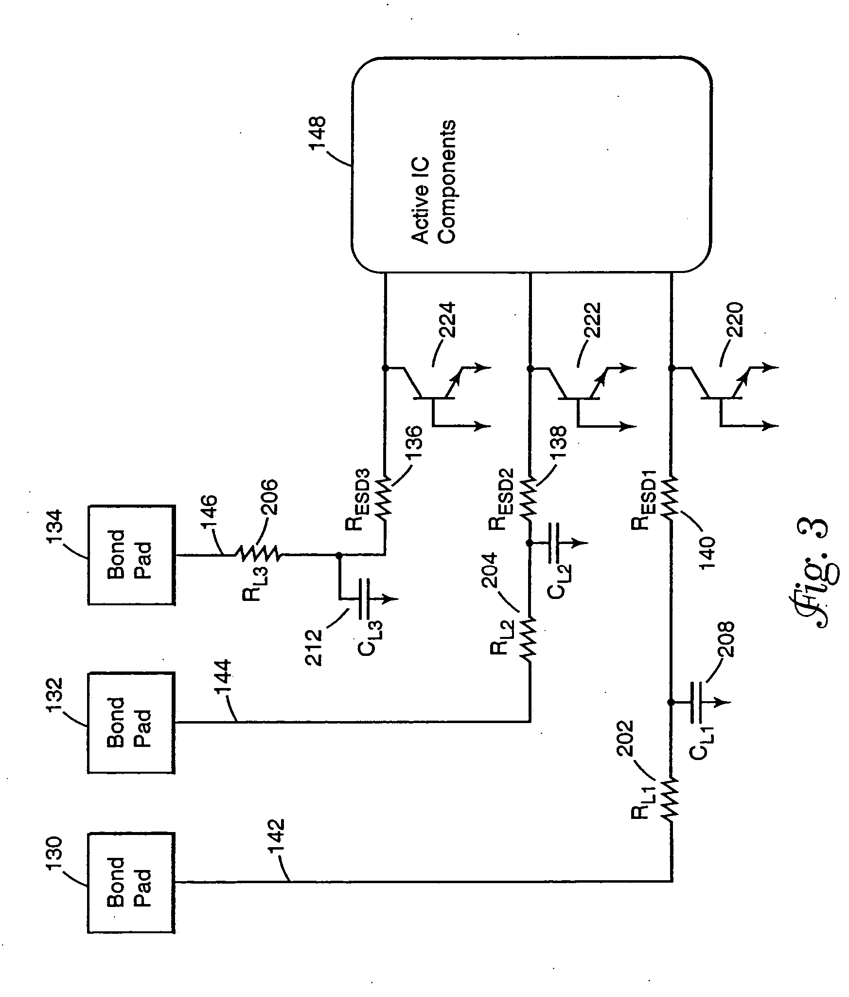
[0022] ESD events can be a problem for all external connections of an integrated circuit and present potentially damaging transients. In this respect both inputs and output circuits are vulnerability points for an integrated circuit, even though the more robus...


PUM


Abstract

An input circuit for an integrated circuit includes an electrostatic discharge circuit. The input circuit incorporates an interconnect pad, an ESD protection resistor, and an interconnect line that are coupled to the active internal components of the integrated circuit. The interconnect pad is coupled to the interconnect line, and the interconnect line is coupled to the ESD protection resistor which is coupled to the active internal components of the integrated circuit. The ESD protection resistor is positioned physically proximate to the active internal components of the integrated circuit and adjusted in value to compensate for the intrinsic resistance or RC time constant of the interconnect line. The circuitry provides for a lower signal propagation delay through the external connection because of lower RC time constants to drive the capacitance of the interconnect.

Description

RELATED APPLICATION [0001] This Application is a Continuation of U.S. application Ser. No. 10 / 704,768 filed Nov. 10, 2003, which is a Continuation of U.S. application Ser. No. 09 / 803,156 filed Mar. 9, 2001, issued as U.S. Pat. No. 6,678,133, on Jan. 13, 2004, both of which are incorporated herein by reference.TECHNICAL FIELD OF THE INVENTION [0002] The invention relates to integrated circuits, and more particularly, to electrostatic discharge protection circuits. BACKGROUND OF THE INVENTION [0003] Electrostatic discharge (ESD) voltage and current can be a major source of damage for integrated circuits. ESD can be a problem with an integrated circuit that is not in operation or coupled to a circuit. At these times, many of the integrated circuit's external connections are floating and exposed to damage. The potential for ESD damage has become even more of a predominant issue with the decreasing device sizes, spacing, and operating voltages of modern components, all of which has the e...

Claims


Application Information

Patent Timeline
Patent Type & Authority Applications(United States)
IPC IPC(8): H01L27/02H02H9/00
CPCH01L27/0288
Inventor ROOHPARVAR, FRANKIE F.
Owner MICRON TECH INC
Why Eureka
Try Eureka