Pwm inverter device

a technology of inverter device and inverter, which is applied in the direction of electric variable regulation, process and machine control, instruments, etc., can solve the problems of complex processing, unstable control characteristic in current control system, and inability to achieve smooth transition switching to a six-step voltage outpu

Inactive Publication Date: 2005-06-16
YASKAWA DENKI KK
View PDF6 Cites 22 Cited by
  • Summary
  • Abstract
  • Description
  • Claims
  • Application Information

AI Technical Summary

Benefits of technology

[0020] Further, complicated processing is not required for implementing processing pertaining to the above means, and the above effects can be obtained only by means of simple processing.

Problems solved by technology

However, as the first related art, an intermediate voltage during a transition from a sinusoidal voltage output to a six-step voltage output cannot be obtained; as a result, there arise problems such that smooth switching between modes is difficult, and that a control characteristic in a current control system, where a current control function is required, becomes unstable during a transitory period of switching.
Further, as the second related art, it has a problem that smooth transition switching to a six-step voltage output requires complicated processing including determination of switching, limitation on lengths of command voltage vectors, or correction of angles of vectors by calculating an arcsine and by reference to a table which stores lengths of vectors and corresponding angles.

Method used


Image

  • Pwm inverter device
  • Pwm inverter device
  • Pwm inverter device

Examples


first embodiment

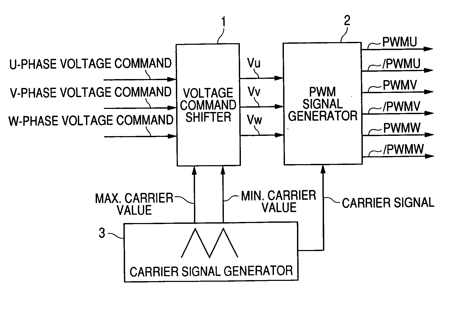
[0046]FIG. 1 is a block diagram of the present invention. 1 denotes a voltage command shifter; 2 denotes a PWM generator; and 3 denotes a carrier signal generator.

[0047] When three-phase voltage commands for U-phase, V-phase and W-phase are supplied from a high-level controller, the voltage command shifter 1 compares absolute values (|Vru|, |Vrv|, |Vrw|) of the respective phase voltage commands (Vru, Vrv, Vrw), and selects a voltage command Vrx of a phase having the largest absolute value among the absolute values. Next, magnitudes of a maximum value (Cmax) and a minimum value (Cmin) of carrier signals obtained from the carrier signal generator 3 are compared with Vrx: [0048] (1) When Vrx is smaller than Cmax, and Vrx is larger than Cmin, [0049] the respective voltage commands are output as signals (Vu, Vv, and Vw) for the PWM generator 2 as they are; [0050] (2) When Vrx is larger than Cmax, (Vrx−Cmax) is calculated, and the following are output: [0051] Vu=Vru−(Vrx-Cmax), Vv=Vrv−(Vr...

second embodiment

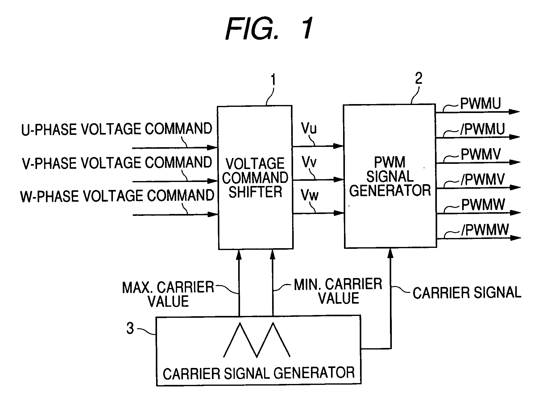
[0057]FIG. 2 is a block diagram of the present invention. 1 denotes a voltage command shifter, 2 denotes a PWM generator, 3 denotes a carrier signal generator, and 4 denotes a voltage command limiter.

[0058] When three-phase voltage commands for U-phase, V-phase and W-phase are supplied from a high-level controller, the voltage command limiter 4 obtains a voltage amplitude of the phase voltage commands, and obtains an amplitude of carrier signals from the maximum value and the minimum value of the carrier signals from the carrier signal generator 3; and the amplitude of the phase voltage commands having an upper limit of 4 / {square root}3 times the amplitude of the carrier signals is supplied to the voltage command shifter 1.

[0059] Operations of the voltage command shifter 1 and the PWM generator 2 are identical with those of the block diagram in FIG. 1.

[0060] When the above limitations are imposed by the high-level controller, the voltage commands can be prevented from becoming exc...

third embodiment

[0061]FIG. 3 is a block diagram of the present invention. 1 denotes a voltage command shifter, 2 denotes a PWM generator, 3 denotes a carrier signal generator, and 5 denotes a voltage command multiplier.

[0062] When three-phase voltage commands for U-phase, V-phase and W-phase are supplied from a high-level controller, the voltage command multiplier 5 obtains an amplitude Vpp of the phase voltage commands, thereby obtaining a maximum carrier signal value Cmax, a minimum value Cmin, and a differential value thereof Cdiff. When the amplitude Vpp of the phase voltage exceeds Cdiff / {square root}3, values (Vu′, Vv′, and Vw′)-which are obtained from multiplication of the respective phase voltage command values (Vru, Vrv, and Vrv) by {square root}3—are supplied to the voltage command shifter 1.

[0063] Operations of the voltage command shifter 1 and the PWM generator 2 are identical with those of the aforementioned block diagram in FIG. 1. Through such operations, linearity of voltage values...


PUM


Abstract

Transition from a sinusoidal wave voltage output to a six-step voltage output involves problems that smooth mode switching is difficult and that switching processing becomes complicated. The present invention provides a PWM inverter having PWM pulse output means (2) for outputting PWM pulse signals upon magnitude comparison of phase voltage commands with a triangular carrier wave. The PWM pulse inverter includes voltage command processing means (1) where a phase whose absolute value is the largest among absolute values of the respective phase voltage commands is selected; values—which in the case where the phase voltage commands are larger than a maximum value of the carrier wave, are differences obtained from subtraction of a maximum value of the carrier wave from the phase voltage commands, or in the case where the phase voltage commands are smaller than a minimum value of the carrier wave, are differences obtained from subtraction of the minimum value of the carrier wave from the phase voltage commands—are subtracted from the respective phase voltage commands; and these results of subtraction are set as the respective output voltage commands; and in other cases, the phase voltage commands are set as phase output voltage commands as they are to thereby be output to the PWM pulse output means (2).

Description

TECHNICAL FIELD [0001] The present invention relates to an inverter servo drive which drives a motor at variable speeds and to a PWM inverter which interconnects systems. BACKGROUND ART [0002] In relation to a PWM inverter which outputs an arbitrary sinusoidal voltage by means of activation / deactivation of an IGBT or the like, there are proposed some signal generating methods for a PWM pulse signal which can serve as a command to activate / deactivate an IGBT or the like. One is a method such as illustrated in FIG. 5, where a PWM pulse signal is generated upon comparison between output voltage commands and a triangular wave (carrier wave) (a triangular wave comparison PWM method), and another is a method where a desired PWM pulse signal is generated by composition of vectors in accordance with a space vector concept (a space vector PWM method). A maximum line voltage (amplitude value) which can be output under the triangular-comparison method using output voltage commands of sinusoida...

Claims


Application Information

Patent Timeline
Patent Type & Authority Applications(United States)
IPC IPC(8): H02M7/48
CPCH02M7/53875H02M7/483H02M7/48H02M7/53846
Inventor YAMANAKA, KATSUTOSHIKANG, JUN-KOOMORIMOTO, SHINYA
Owner YASKAWA DENKI KK
Why Eureka
Try Eureka