Extendable method for revising patterned microelectronic conductor layer layouts

a technology of microelectronic conductors and extendable methods, which is applied in the direction of electric digital data processing, instruments, computing, etc., can solve the problems of time-consuming and iterative methods, and achieve the effect of being ready for commercial implementation

Inactive Publication Date: 2005-06-16
TAIWAN SEMICON MFG CO LTD
View PDF19 Cites 1 Cited by
  • Summary
  • Abstract
  • Description
  • Claims
  • Application Information

AI Technical Summary

Benefits of technology

[0014] A second object of the present invention is to provide the method for designing the patterned microelectronic conductor layer layout in accord with the first object of the present invention and a system for designing the patterned microelectronic conductor layer layout in accord with the first object of the present invention, wherein the patterned microelectronic conductor layer layout is efficiently designed.
[0015] A third object of the present invention is to provide a method for designing the patterned microelectronic conductor layer layout in accord with the first object of the present invention and the second object of the present invention and a system for designing the patterned microelectronic conductor layer layout in accord with the first object of the present invention and the second object of the present invention, wherein the method is readily commercially implemented.
[0019] There is provided by the present invention a method for designing a patterned microelectronic conductor layer layout for use when fabricating a microelectronic fabrication and a system for designing the patterned microelectronic conductor layer layout for use when fabricating the microelectronic fabrication, wherein the patterned microelectronic conductor layer layout is efficiently designed while employing the method for designing the patterned microelectronic conductor layer layout and the system for designing the patterned microelectronic conductor layer layout.
[0020] The present invention realizes the foregoing object by providing within each wiring layout record within a series of wiring layout records within a wiring layout database directed towards a series of microelectronic fabrications an unoccupied equivalent wiring location within which may be formed at least one optional wiring pattern. Thus, when there is designed within an unoccupied equivalent wiring location for a single wiring layout record within the series of wiring layout records (as directed towards a single microelectronic fabrication within the series of microelectronic fabrications) at least one optional wiring pattern and an interconnect option to the at least one optional wiring pattern, the same at least one optional wiring pattern and interconnect option to the at least one optional wiring pattern may be incorporated into the remaining unoccupied equivalent wiring locations within the remaining wiring layout records within the wiring layout database (to efficiently extend the wiring modification from the single microelectronic fabrication to the series of microelectronic fabrications).
[0022] The present invention employs microelectronic layer design tools, microelectronic layer layout tools and database manipulation tools as are otherwise generally conventional in the microelectronic fabrication art for designing microelectronic fabrications as are otherwise generally conventional in the microelectronic fabrication art, but employed within the context of a series of specific design and operational limitations which provide at least in part the present invention. Since it is at least in part a series of design and operational limitations which provides at least in part the present invention, rather than the existence of methods and materials which provides the present invention, the method of the present invention is readily commercially implemented.

Problems solved by technology

While such iterative methods do in fact provide an optimized patterned microelectronic conductor layer layout which in turn provides an enhanced microelectronic fabrication performance, such iterative methods are often time consuming, in particular when employed for optimizing a library of patterned microelectronic conductor layer layouts which is employed within a corresponding library of related microelectronic fabrications such as to in turn optimize performance of the corresponding library of related microelectronic fabrications.

Method used


Image

  • Extendable method for revising patterned microelectronic conductor layer layouts
  • Extendable method for revising patterned microelectronic conductor layer layouts
  • Extendable method for revising patterned microelectronic conductor layer layouts

Examples


Embodiment Construction

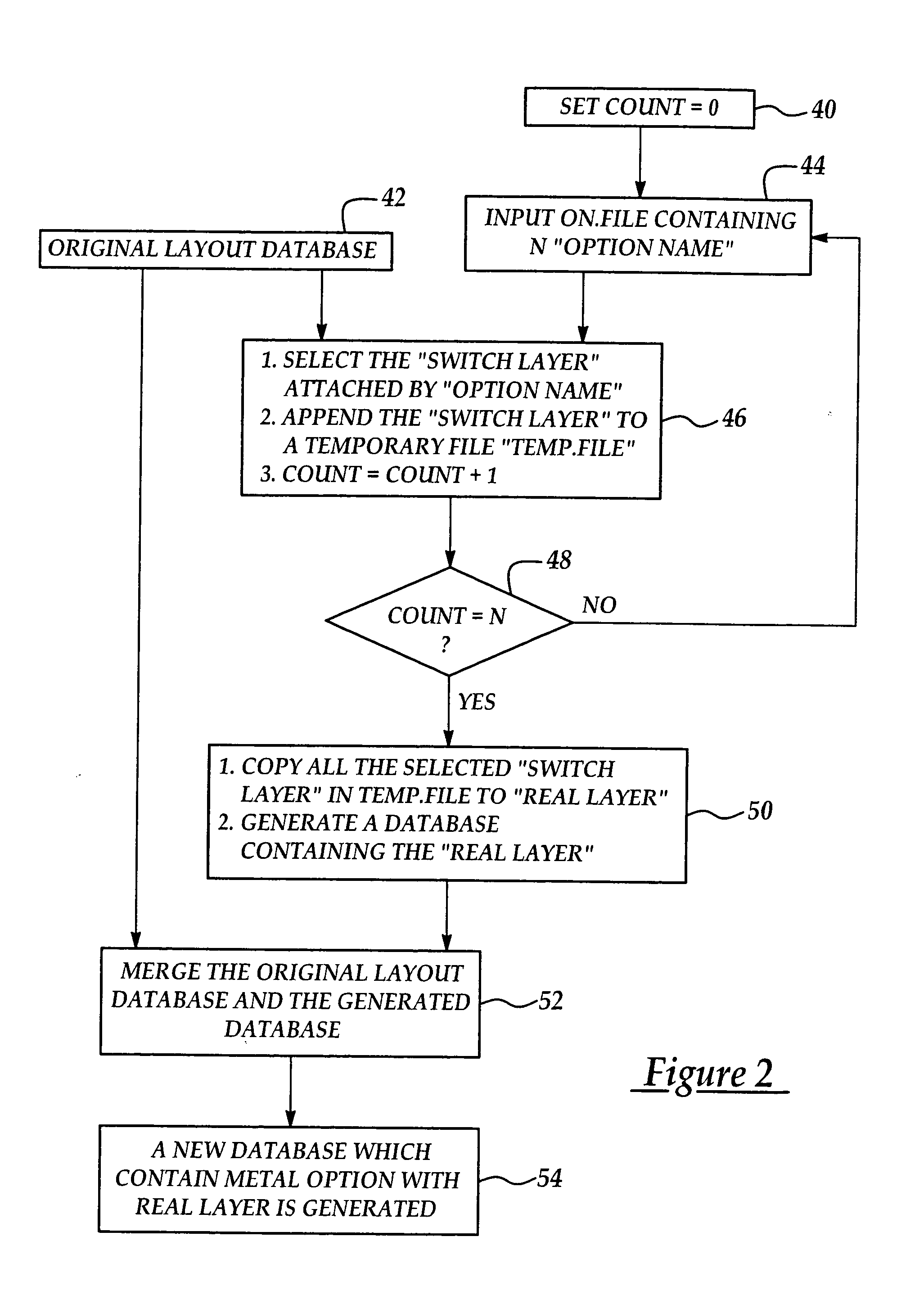
[0029] There is provided by the present invention a method for designing a patterned microelectronic conductor layer layout for use when fabricating a microelectronic fabrication and a system for designing the patterned microelectronic conductor layer layout for use when fabricating the microelectronic fabrication, wherein the patterned microelectronic conductor layer layout is efficiently designed while employing the method for designing the patterned microelectronic conductor layer layout and the system for designing the patterned microelectronic conductor layer layout.

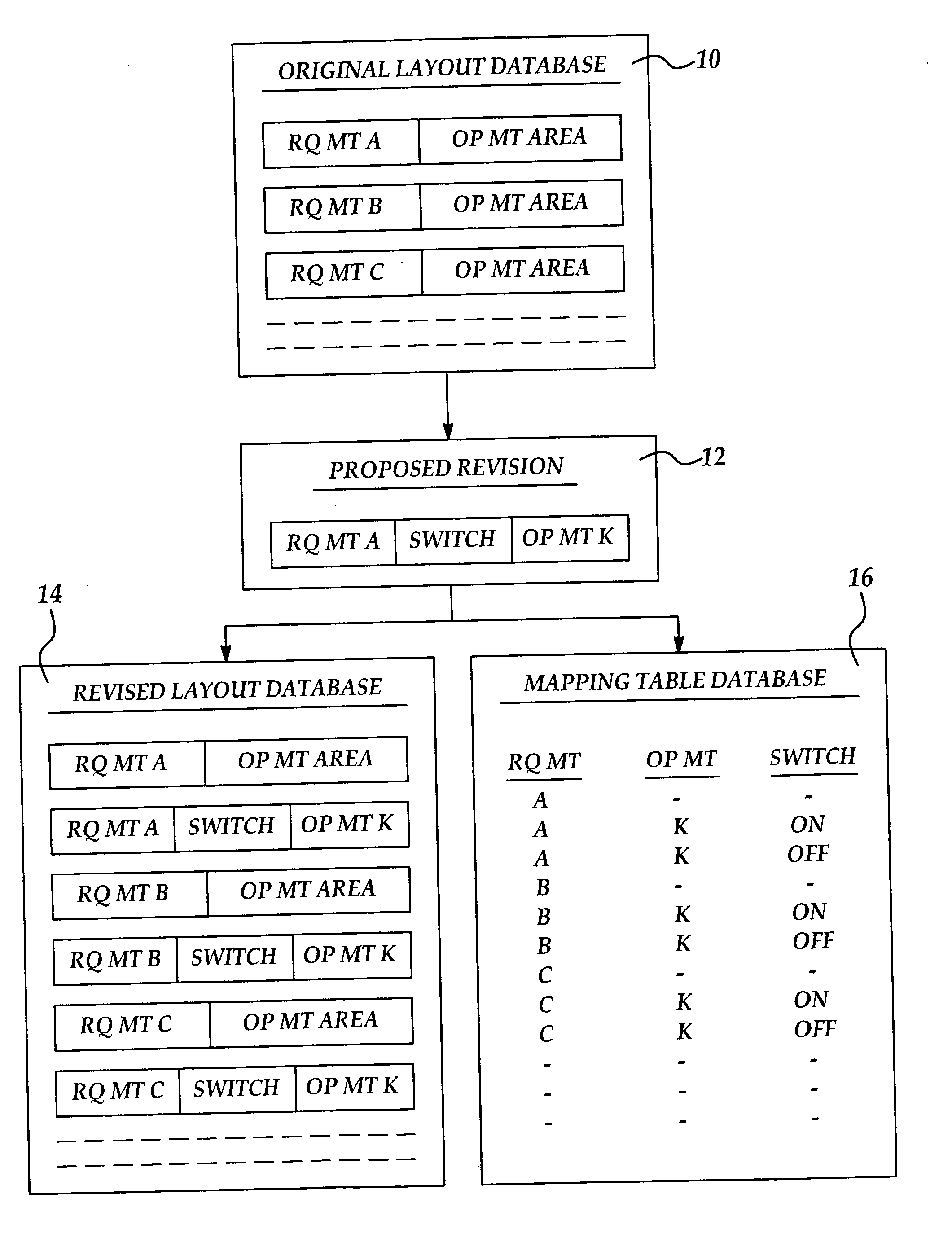
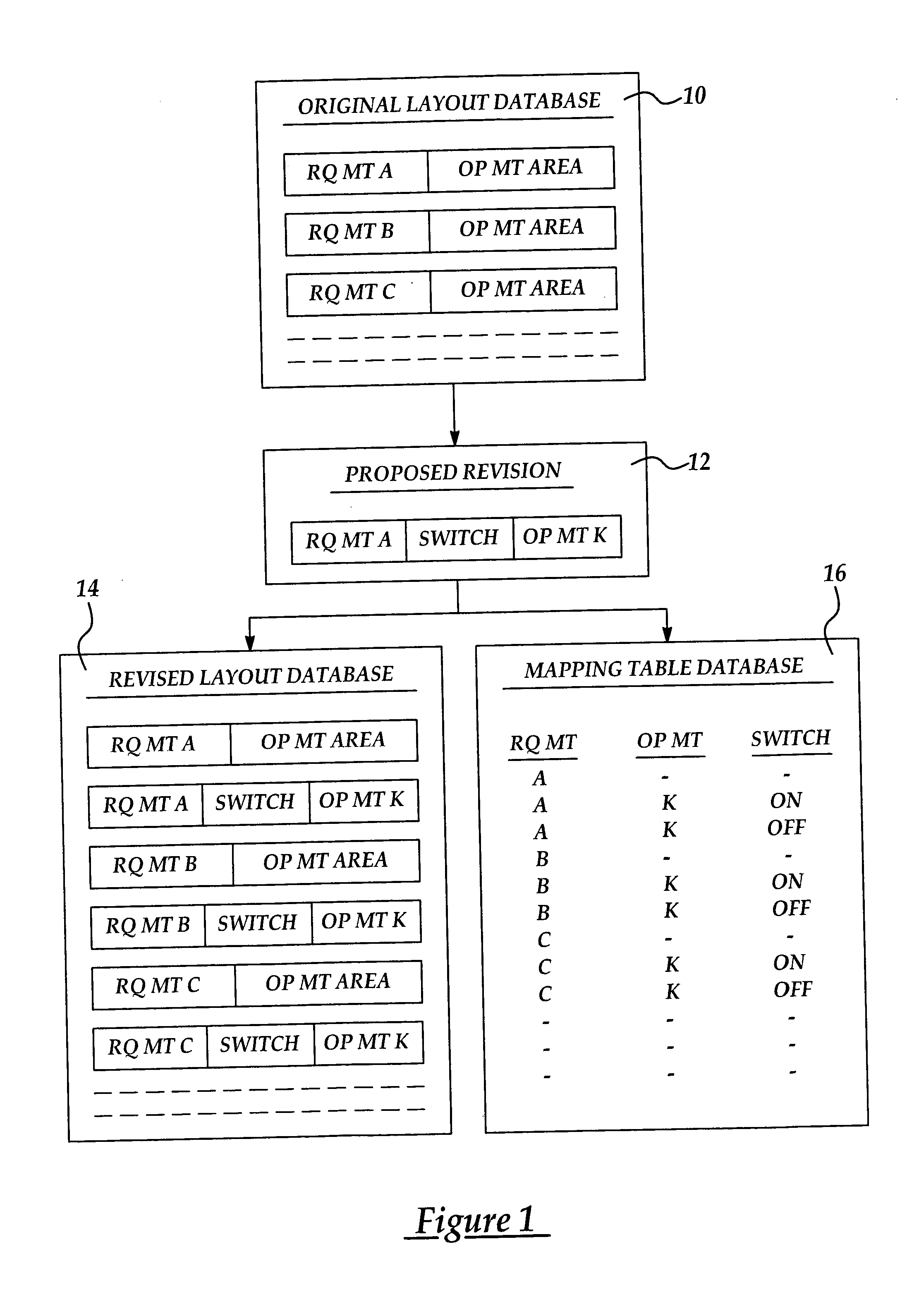
[0030] The present invention realizes the foregoing object by providing within each wiring layout record within a series of wiring layout records within a wiring layout database directed towards a series of microelectronic fabrications an unoccupied equivalent wiring location within which may be formed at least one optional wiring pattern. Thus, when there is designed within an unoccupied equivalent wiring location...


PUM


Abstract

Within both a method for revising a patterned conductor layer and a system for revising the patterned conductor layer there is provided within each wiring layout record within a series of wiring layout records within a wiring layout database directed towards a series of microelectronic fabrications an unoccupied equivalent wiring location within which may be formed at least one optional wiring pattern. When there is designed within an unoccupied equivalent wiring location for a single wiring layout record within the series of wiring layout records at least one optional wiring pattern and an interconnect option to the at least one optional wiring pattern.

Description

BACKGROUND OF THE INVENTION [0001] 1. Field of the Invention [0002] The present invention relates generally to methods for revising patterned conductor layer layouts employed for fabricating microelectronic fabrications. More particularly, the present invention relates to methods for efficiently revising patterned conductor layer layouts employed for fabricating microelectronic fabrications. [0003] 2. Description of the Related Art [0004] Microelectronic fabrications are formed from microelectronic substrates over which are formed patterned microelectronic conductor layers which are separated by microelectronic dielectric layers. [0005] Integral to the fabrication of patterned microelectronic conductor layers within microelectronic fabrications is the design and development of patterned microelectronic conductor layer layouts employed for fabricating patterned microelectronic conductor layers within microelectronic fabrications. Such patterned microelectronic conductor layer layouts...

Claims


Application Information

Patent Timeline
Patent Type & Authority Applications(United States)
IPC IPC(8): G06F9/45G06F17/50
CPCG06F17/5077G06F30/394
Inventor CHEN, HSIAO-HUIKUO, CHENG-HSIUNG
Owner TAIWAN SEMICON MFG CO LTD
Why Eureka
Try Eureka