Semiconductor memory devices and semiconductor packages

a memory device and semiconductor technology, applied in the field of semiconductor devices, can solve problems such as power consumption in these memory devices, and achieve the effects of reducing power consumption, high performance, and increasing operational frequency

Active Publication Date: 2011-08-11
SAMSUNG ELECTRONICS CO LTD
View PDF4 Cites 65 Cited by
  • Summary
  • Abstract
  • Description
  • Claims
  • Application Information

AI Technical Summary

Benefits of technology

[0008]Some example embodiments provide a wide input-output semiconductor memory device having a multi-channel interface and having high performance with relatively low power consumption.
[0036]The semiconductor memory device according to example embodiments may have a multi-channel and wide input-output interface and thus the semiconductor memory device according to example embodiments may reduce power consumption with an increase of operational frequency, and simultaneously support a processor of high performance.
[0037]The semiconductor memory device according to example embodiments may have the input-output bump pad part formed in the central region of the semiconductor die, and thus the semiconductor memory device according to example embodiments may be conveniently coupled to other devices or chips of various structures or the layout may be easily modified depending on changes of manufacturing process.
[0038]The semiconductor memory device according to example embodiments may include the support bump pad part located in marginal or edge regions of the semiconductor die, thereby enhancing the reliability of a chip-on-chip packaging arrangement.
[0039]In the semiconductor memory device according to example embodiments, the plurality of memory cell arrays, the plurality of channel bump pad and / or some of the peripheral circuits may be designed using mirror images or shifted images, thereby effectively designing the semiconductor memory device and minimizing process variation.

Problems solved by technology

In addition, there is a need for a reduction in power consumption in these memory devices due to limited battery capacity in portable devices.

Method used


Image

  • Semiconductor memory devices and semiconductor packages
  • Semiconductor memory devices and semiconductor packages
  • Semiconductor memory devices and semiconductor packages

Examples


Embodiment Construction

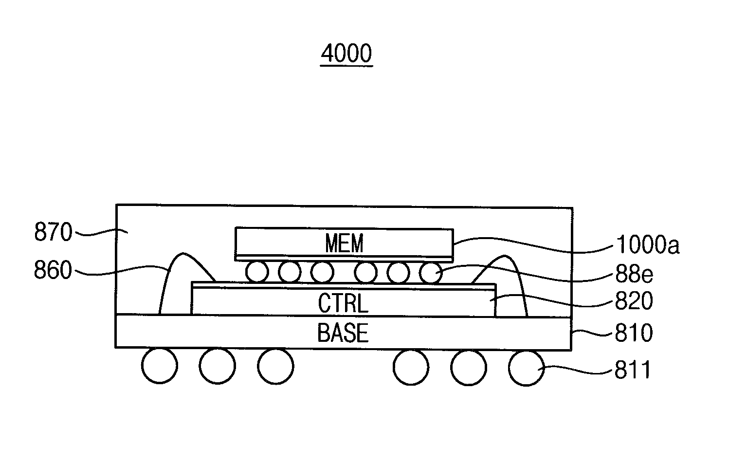
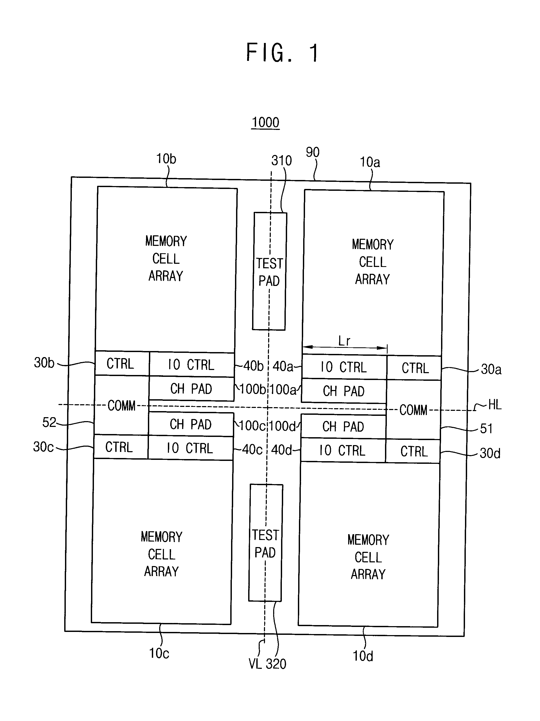
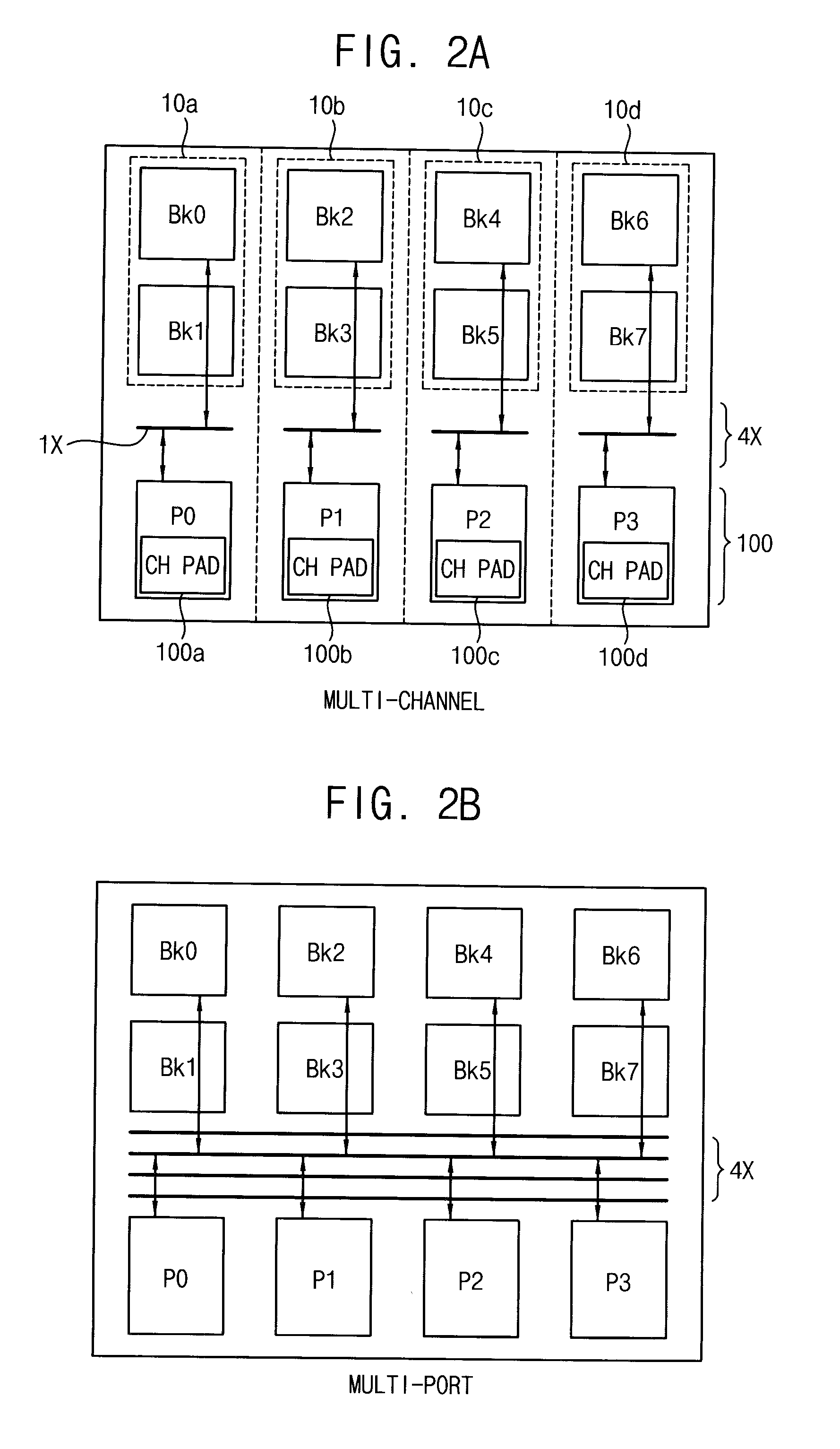
[0054]Various example embodiments will be described more fully hereinafter with reference to the accompanying drawings, in which some example embodiments are shown. The present inventive concept may, however, be embodied in many different forms and should not be construed as limited to the example embodiments set forth herein. Rather, these example embodiments are provided so that this disclosure will be thorough and complete, and will fully convey the scope of the present inventive concept to those skilled in the art. In the drawings, the sizes and relative sizes of layers and regions may be exaggerated for clarity. Like numerals refer to like elements throughout.

[0055]It will be understood that, although the terms first, second, third, etc. may be used herein to describe various elements, these elements should not be limited by these terms. These terms are used to distinguish one element from another. Thus, a first element discussed below could be termed a second element without d...


PUM


Abstract

A semiconductor memory device includes a semiconductor die and an input-output bump pad part. The semiconductor die includes a plurality of memory cell arrays. The input-output bump pad part is formed in a central region of the semiconductor die. The input-output bump pad part provides a plurality of channels for connecting each of the memory cell arrays independently to an external device. The semiconductor memory device may adopt the multi-channel interface, thereby having high performance with relatively low power consumption.

Description

CROSS-REFERENCE TO RELATED APPLICATIONS[0001]This U.S. non-provisional application claims the benefit of priority under 35 USC §119 to U.S. Provisional Application No. 61 / 302,773 filed on Feb. 9, 2010 in the USPTO, and Korean Patent Application No. 10-2010-0018362 filed on Mar. 2, 2010 in the Korean Intellectual Property Office (KIPO), the contents of each of which are herein incorporated by reference in their entirety for all purposes as if fully set forth herein.BACKGROUND[0002]1. Technical Field[0003]Example embodiments relate to semiconductor devices, and more particularly to semiconductor memory devices and semiconductor packages having a multi-channel interface.[0004]2. Description of the Related Art[0005]Various interfaces have been developed to provide a semiconductor memory device having high performance with relatively low power consumption. Recently, the low power double data rate 2 (LPDDR2) standard has been adopted to support portable devices such as a mobile phone, a s...

Claims


Application Information

Patent Timeline
Patent Type & Authority Applications(United States)
IPC IPC(8): H01L27/118
CPCG11C5/025H01L27/108H01L2224/16145H01L2224/16225H01L2224/32225H01L2224/48227H01L2224/73207H01L2224/73265H01L2924/15311G11C5/06H01L24/09H01L25/0657H01L27/0255H01L2225/06541H01L2224/0912H01L2224/09179H01L2224/09515H01L22/32H01L2224/0401H01L2924/00012H01L2924/00H01L24/73H01L2224/16146H01L2224/17181H01L2224/13025H10B12/00
Inventor LEE, HO-CHEOLOH, CHI-SUNGKIM, JIN-KUK
Owner SAMSUNG ELECTRONICS CO LTD
Why Eureka
Try Eureka