Thermally enhanced semiconductor package

Active Publication Date: 2005-06-23
TEXAS INSTR INC
View PDF7 Cites 30 Cited by
  • Summary
  • Abstract
  • Description
  • Claims
  • Application Information

AI Technical Summary

Benefits of technology

[0014] Thermal dissipation from the chip is primarily through the semiconductor chip backside and into the heat sink where it is spread across the width of the sink, through the base, and into the PCB. A solid conductive metal heat sink introduces only a single thermal barrier, i.e. the adhesive, between the chip and sink, whereas, conventional heat dissipation techniques may include multiple interfaces and thermal barriers. The heat sink construction of a single piece of material lends itself to rapid thermal response and thereby supports reliable chip operation.
[0015] In addition t

Problems solved by technology

Circuits used in telecommunications and other applications may dissipate power in excess of several Watts.
However, such structures add considerably to the package size, the amount of board space required, and to costs.
With the continued drive towards reducing the dimensions of integrated circuit packages, conventional packaging techniques

Method used


Image

  • Thermally enhanced semiconductor package
  • Thermally enhanced semiconductor package
  • Thermally enhanced semiconductor package

Examples


Example

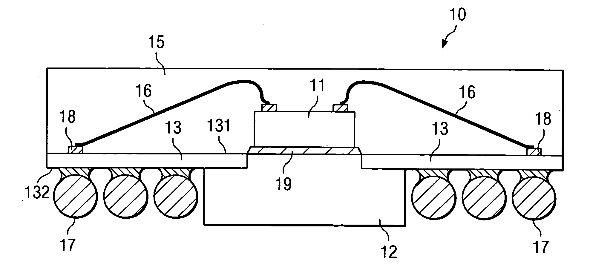
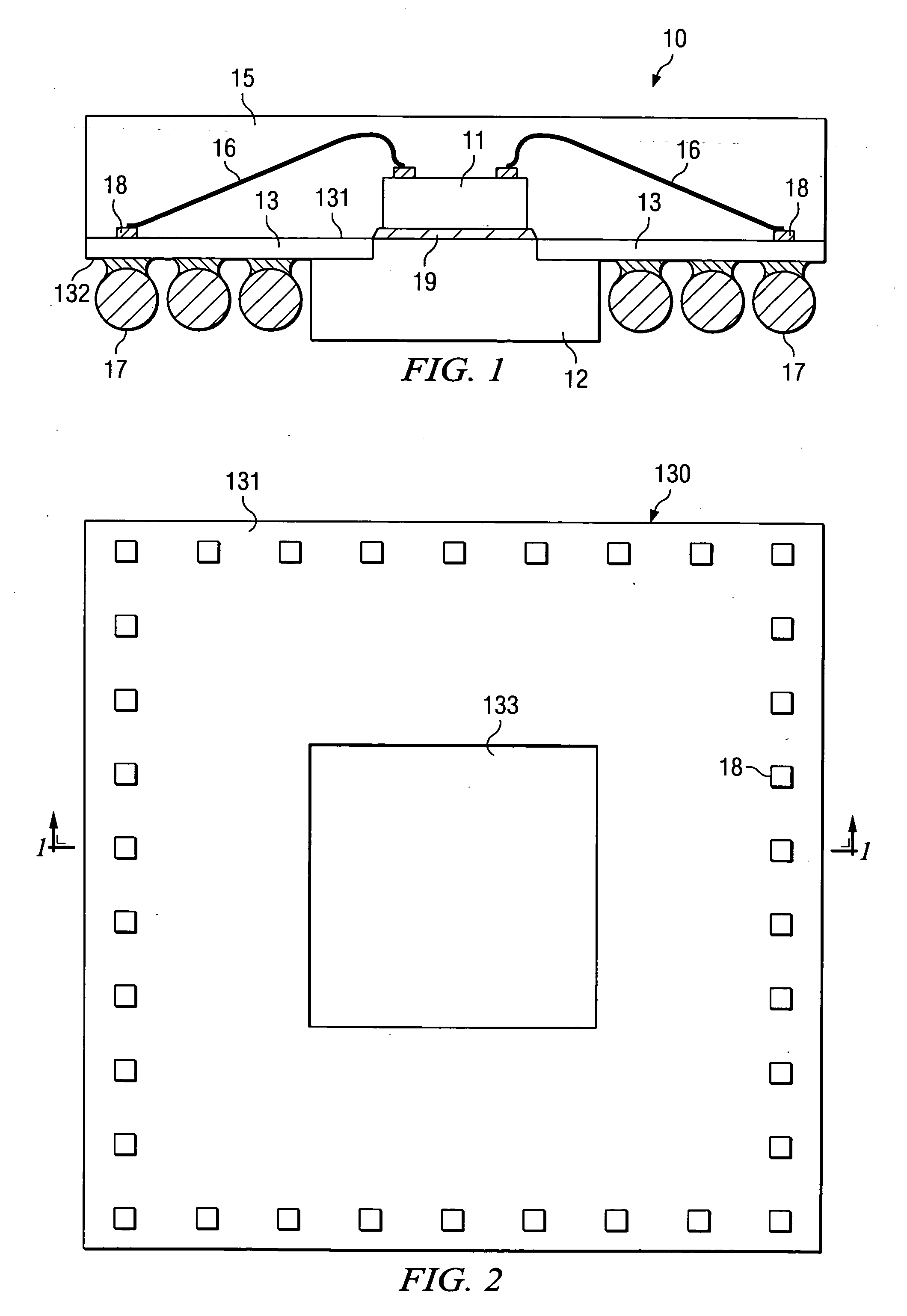
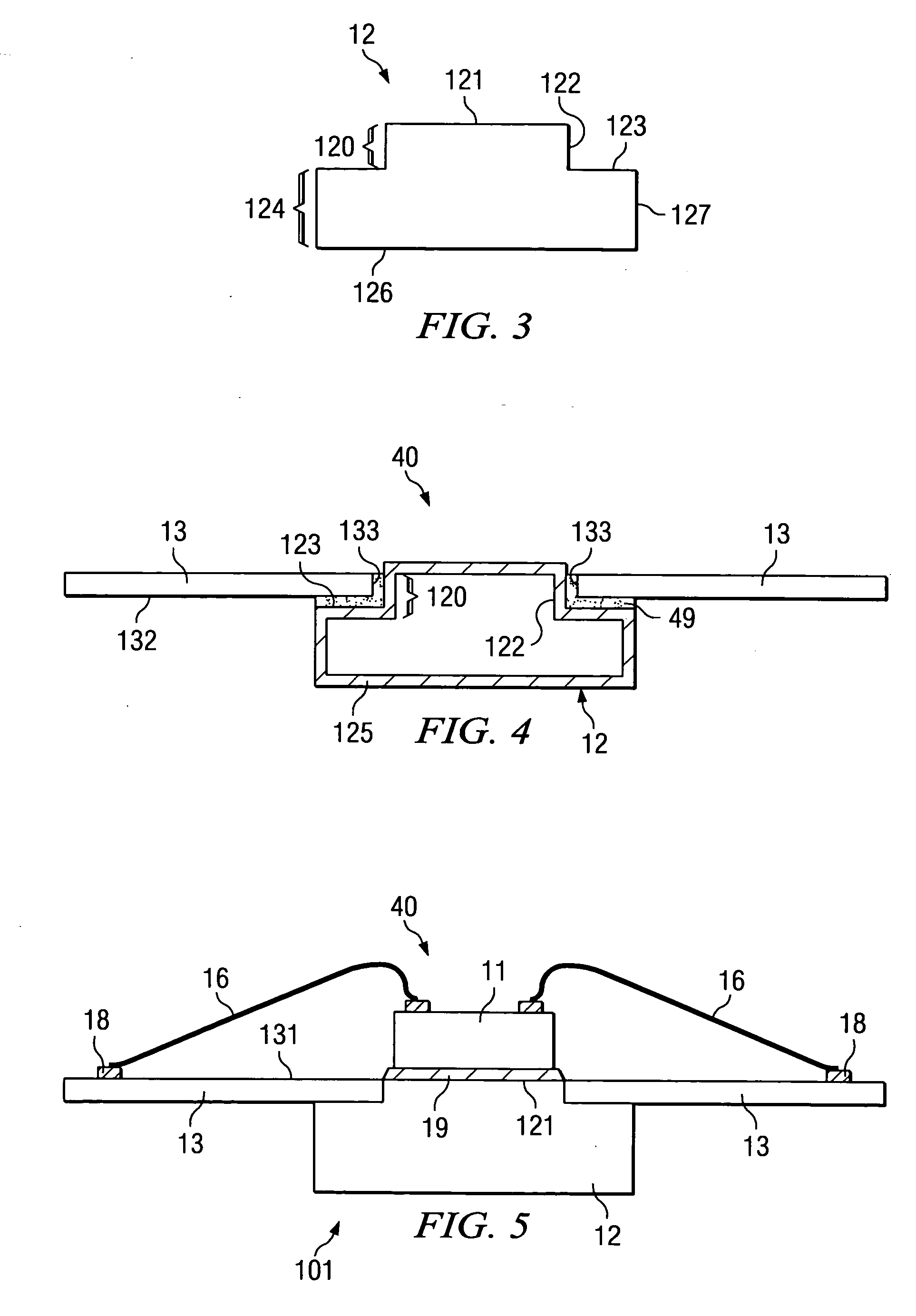
[0046] In FIG. 9, a second embodiment of thermally enhanced BGA package 90 includes semiconductor chip 91 adhered to the first horizontal surface 921 of a “T” shaped heat sink 92 by a thermally conductive adhesive 99, substrate 93 having a window through which the vertical trunk 922 of the “T” shaped heat sink extends, a plurality of bond pads 935 on the first surface 931, and an array of solder balls 94 on the second surface 932. Chip 91, bond wires 96, and first surface 931 of the substrate are encapsulated in a thermosetting molding compound 98. Heat dissipated by the chip is spread across the horizontal section of the heat sink 92 and into the vertical trunk 922 for further dissipation into a PBC or alternate heat sink. Materials of construction and processes are similar to those described for the first embodiment of the thermally enhanced BGA device. The heat sink trunk 922 is aligned through the window in the substrate 93 and the top portion of the “T” shaped sink 92 is adhere...


PUM


Abstract

A thermally enhanced BGA semiconductor device 10 having a heat sink 12 formed from a single piece of material with an expanded base and a pedestal in contact with a semiconductor chip 11. The pedestal is aligned through a window opening in a substrate 13 and the top surface of the base is adhered to the substrate. The heat sink 12 with an expanded base provides a path for rapid and efficient heat spreading and dissipation, a stand-off and an aid to improved package planarity during reflow to a PCB, and a long path for ingress of contaminants into the package. The device is amenable to high volume, low cost production.

Description

FIELD OF THE INVENTION [0001] The invention relates generally to a semiconductor device, and more specifically to a thermally enhanced semiconductor package; and to a method of fabrication. BACKGROUND OF THE INVENTION [0002] An integrated circuit package provides electrical connections from an integrated circuit chip to external conductors, and protection of the chip from environmental conditions. Additionally, management of thermal dissipation is an increasingly important consideration in the development of packages for many integrated circuit chips. Circuits used in telecommunications and other applications may dissipate power in excess of several Watts. Consequently, it is necessary to provide an integrated circuit package having an efficient method of heat removal. Typically a heat sink for an integrated circuit is provided by mounting the chip in contact with a thermally conductive metal or alloy structure having at least one surface exposed to the ambient environment or to a s...

Claims


Application Information

Patent Timeline
IPC IPC(8): H01L23/367H01L23/498H05K1/02
CPCH01L23/3677H01L2924/15151H01L24/45H01L2224/32188H01L2224/45144H01L2224/48091H01L2224/48472H01L2924/01079H01L2924/14H01L2924/30107H05K1/0204H05K2201/09781H05K2201/10734H05K2201/10969H05K2201/2036H01L23/49816H01L2224/73265H01L2924/01013H01L24/48H01L2924/00014H01L2924/00H01L2924/181H01L2924/00012
Inventor WOODALL, JOE D.MORTAN, ROBERT F.
Owner TEXAS INSTR INC
Why Eureka
Try Eureka