
Circuit arrangement and method for driving electronic chips

Inactive Publication Date: 2005-06-23
POLARIS INNOVATIONS
View PDF4 Cites 2 Cited by
  • Summary
  • Abstract
  • Description
  • Claims
  • Application Information

AI Technical Summary

Benefits of technology

[0012] One advantage of the present invention is that circuit units to be tested in a test apparatus can be individually addressed without circuit units which are not intended to be addressed having to be removed from a supply voltage.
[0013] A further advantage is that repair work on individual chips which are jointly arranged and introduced into the test apparatus is easier to accomplish. Circuit units to be tested are advantageously repaired by means of e-fuse self-repair techniques, for example.
[0014] It is also useful that predeterminable command blocks can be applied to specific circuit units to be tested in order to carry out individual test sequences. The advantage of a high degree of parallelism during testing by machine is retained in this case since command sequences can be applied in parallel to all of the circuit units to be tested. The decision as to which command sequence is relevant to a specific circuit unit to be tested is made using a specific identification unit which is assigned to the corresponding circuit unit to be tested.
[0015] In one embodiment of the invention, there is a method for testing circuit units to be tested in a test apparatus based on an assignment of different identification units to the circuit units to be tested, including:
[0016] a) connection of the circuit units to be tested to the test apparatus;
[0017] b) outputting of a tester data stream containing command blocks from the test apparatus;

Problems solved by technology

The increasing integration density and also the progressive complexity of electronic circuit units (electronic chips) result in increased requirements when testing these circuit units.
Individual addressing of individual electronic chips disadvantageously conflicts with increasing the parallelism of testing and thus shortening the test duration.
Disadvantageously, this concept is not suitable for future test setups since parallelism of the voltage supply must also be provided, that is to say future test setups will provide supply voltage sources for a plurality of electronic chips, with the result that this type of selective addressing will not be able to be carried out.
Economically, it is problematical that the test costs are taking up an ever increasing portion of the production costs.
However, the conventional methods disadvantageously no longer allow the individual electronic chip to be tested to be individually addressed.
This fact prevents future requirements from being met in the case of e-fuse self-repair of memory modules or in the case of individual driver calibration (OCD) of DDR (Double Data Rate) II technology, in which individual addressing of electronic chips—together with highly parallel measurement at the same time—is absolutely necessary.

Method used


Image

  • Circuit arrangement and method for driving electronic chips
  • Circuit arrangement and method for driving electronic chips

Examples


Embodiment Construction

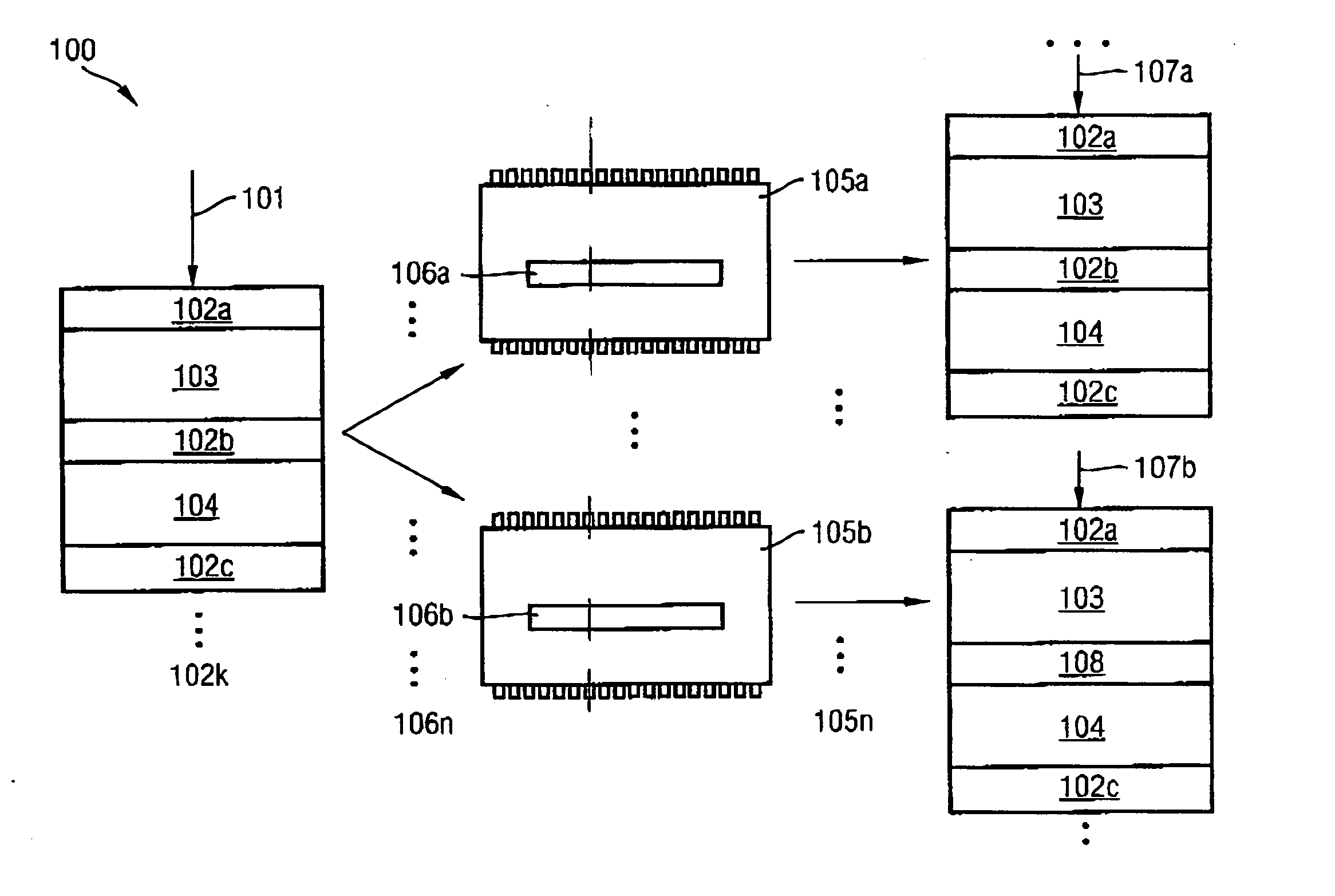
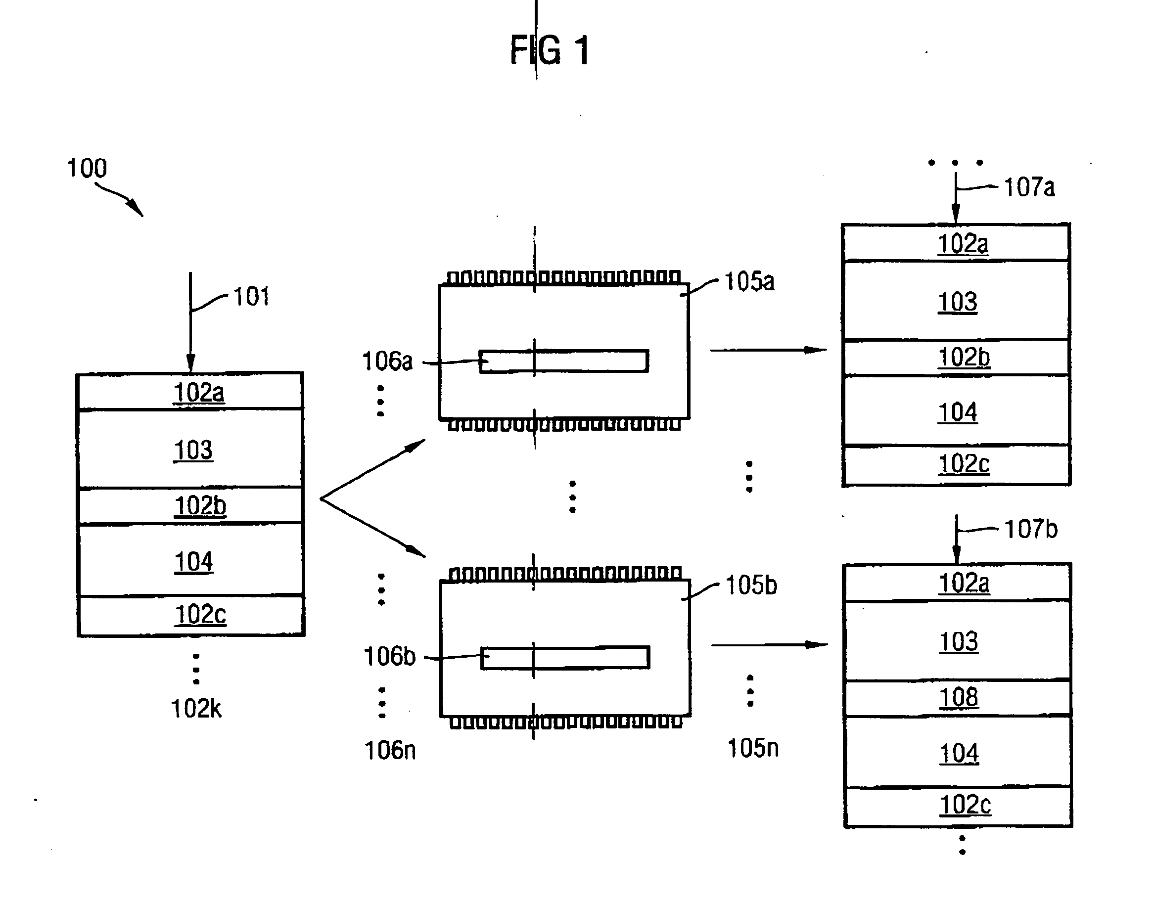
[0044] The block diagram shown in FIG. 1 illustrates how the components of a test apparatus 100 for testing circuit units 105a, 105b, . . . 105i, . . . 105n to be tested. In this exemplary embodiment, it shall be assumed that the total number of circuit units 105-105n to be simultaneously tested in parallel is n.

[0045] It should be pointed out that “i” is used to denote a running index, that is to say i=a, b, . . . n. In the preferred exemplary embodiment of the present invention shown in FIG. 1, a tester data stream 101 is provided by the test apparatus via an output device (not shown) of the test apparatus 100. Said tester data stream 101 preferably includes different command blocks 102a, 102b, 102c, 102i, . . . 102k. In this exemplary embodiment, the number of command blocks is k, k being a variable integer. “i” in turn represents a running index, that is to say i=a, b, c, . . . i, . . . k.

[0046] Individual command blocks 102a-102k are assigned to the individual circuit units 1...


PUM


Abstract

The invention provides a method for testing circuit units to be tested in a test apparatus, different identification units being assigned to the circuit units to be tested, the circuit units to be tested being connected to the test apparatus, a tester data stream including command blocks being output from the test apparatus, the tester data stream being compared with the identification units, the circuit unit to be tested, the identification unit of which matches the tester data stream output by the test apparatus, being activated and at least one command block for this circuit unit to be tested being processed in the circuit unit to be tested, whereupon the circuit unit to be tested is deactivated.

Description

CLAIM FOR PRIORITY [0001] This application claims the benefit of priority to German Application No. 103 24 080.2, filed on May 27, 2003 in the German language, the contents of which are hereby incorporated by reference. TECHNICAL FIELD OF THE INVENTION [0002] The present invention relates to the testing of electronic circuit units (electronic chips) with the aid of testers, and in particular, to the individual testing of individual electronic. BACKGROUND OF THE INVENTION [0003] The increasing integration density and also the progressive complexity of electronic circuit units (electronic chips) result in increased requirements when testing these circuit units. At present, up to 256 electronic chips are simultaneously introduced into a test device (tester) and tested by machine. In this case, there are typically 66 connection pins (pins) per electronic chip. [0004] Test signals or test sequences are applied to specific pins and an output signal (actual signal) which is reproduced by t...

Claims


Application Information

Patent Timeline
IPC IPC(8): G01R31/317G11C29/16
CPCG01R31/31723G11C2029/4402G11C29/4401G11C29/16
Inventor FLACH, BJORNLOGISCH, ANDREASRUF, WOLFGANGSCHITTENHELM, MICHAELSCHNELL, MARTIN
Owner POLARIS INNOVATIONS
Learn More