Non-volatile memory device and fabricating method thereof

a memory device and non-volatile technology, applied in the direction of semiconductor devices, electrical devices, transistors, etc., can solve the problems of difficulty in carrying out etching processes, and achieve the effect of raising the coupling ratio without lowering the degree of integration

Inactive Publication Date: 2005-06-30
DONGBU ELECTRONICS CO LTD
View PDF6 Cites 26 Cited by
  • Summary
  • Abstract
  • Description
  • Claims
  • Application Information

AI Technical Summary

Benefits of technology

[0016] An object of the present invention is to provide a non-volatile memory device and fabricating method thereof, in which a height o

Problems solved by technology

In case a height of the floating gate conductor layer pattern 10

Method used


Image

  • Non-volatile memory device and fabricating method thereof
  • Non-volatile memory device and fabricating method thereof
  • Non-volatile memory device and fabricating method thereof

Examples


Embodiment Construction

[0033] Reference will now be made in detail to the preferred embodiments of the present invention, examples of which are illustrated in the accompanying drawings. Wherever possible, the same reference numbers will be used throughout the drawings to refer to the same or like parts.

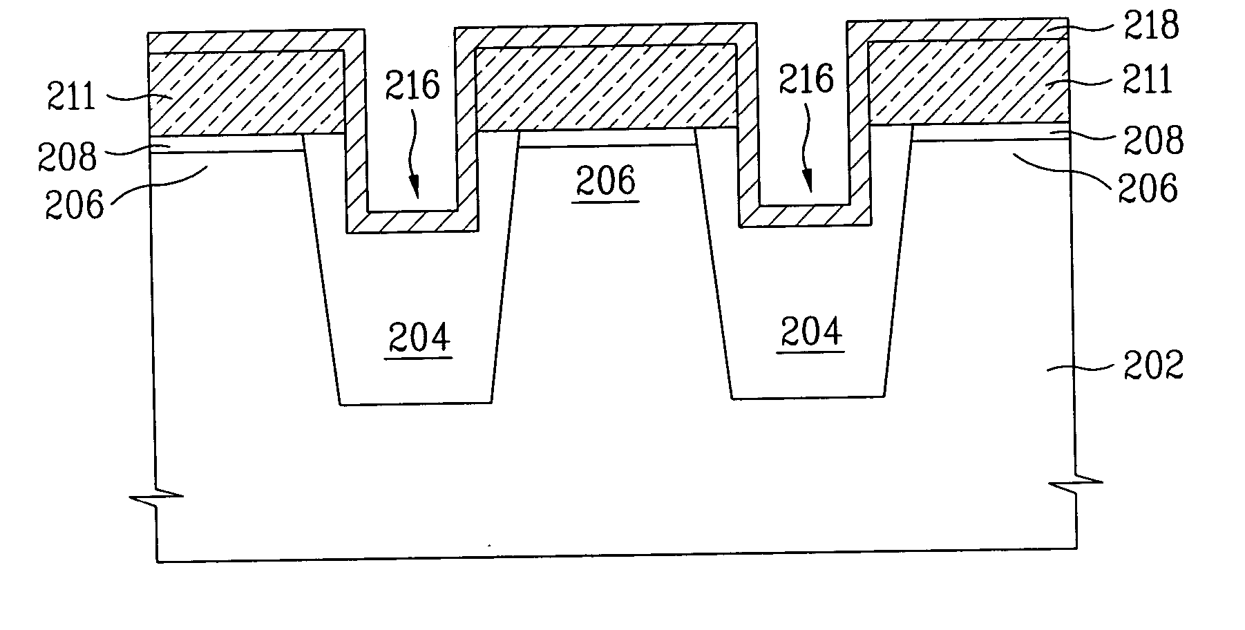
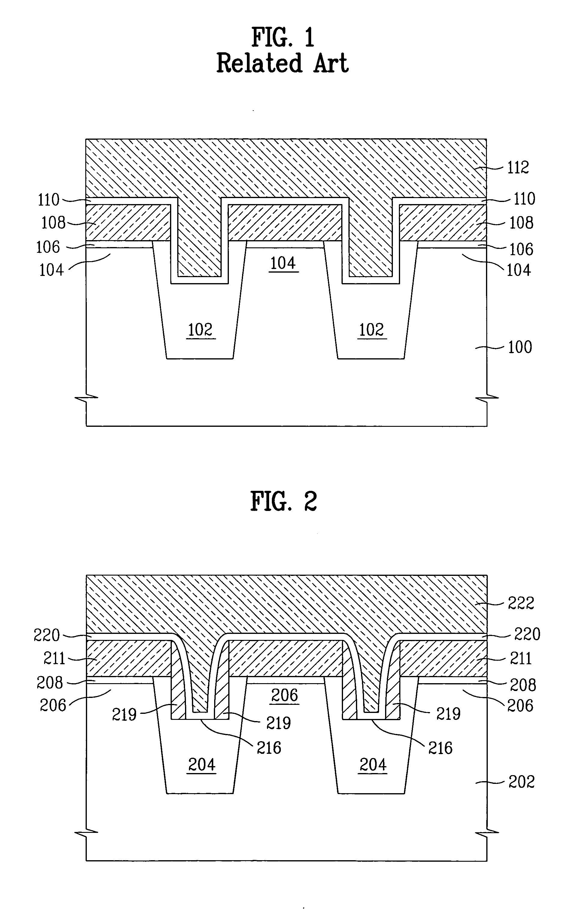
[0034]FIG. 2 is a cross-sectional diagram of a non-volatile memory device according to the present invention.

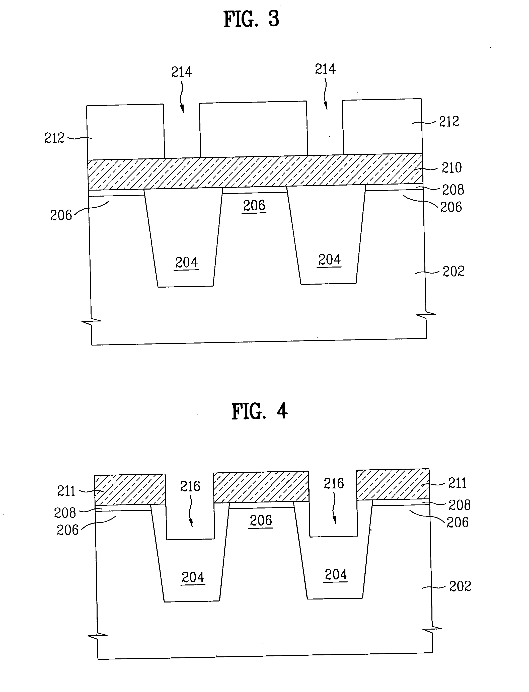
[0035] Referring to FIG. 2, a tunnel oxide layer pattern 208 is arranged on an active area 206 of a semiconductor substrate 202 defined by a device isolation layer 204.

[0036] The device isolation layer 104 has a trench shape and a recess 216 having a prescribed depth is formed on a top of the device isolation layer 204. And, the depth of the recess 216 is about 300˜2,000 Å.

[0037] A floating gate conductor layer pattern 211 is arranged on the tunnel oxide layer 208.

[0038] A conductive gate spacer layer 219 is provided to sidewalls of the floating gate conductor layer pattern 211 and the recess 21...


PUM


Abstract

The present invention provides a non-volatile memory device and fabricating method thereof, in which a height of a floating gate conductor layer pattern is sustained without lowering a degree of integration and by which a coupling ratio is raised. The present invention includes a trench type device isolation layer defining an active area within a semiconductor substrate, a recess in an upper part of the device isolation layer to have a prescribed depth, a tunnel oxide layer on the active area of the semiconductor substrate, a floating gate conductor layer pattern on the tunnel oxide layer, a conductive floating spacer layer provided to a sidewall of the floating gate conductor layer pattern and a sidewall of the recess, a gate-to-gate insulating layer on the floating fate conductor layer pattern and the conductive floating spacer layer, and a control gate conductor layer on the gate-to-gate insulating layer.

Description

[0001] This application claims the benefit of the Korean Application No. P2003-0098355 filed on Dec. 27, 2003, which is hereby incorporated by reference. BACKGROUND OF THE INVENTION [0002] 1. Field of the Invention [0003] The present invention relates to a non-volatile memory device and fabricating method thereof, and more particularly, to a non-volatile memory device having a high coupling ratio and fabricating method thereof. [0004] 2. Discussion of the Related Art [0005] Generally, semiconductor memory devices are categorized into a volatile memory device, which loses data in case of cutting off power supply, such as DRAM (dynamic random access memory) and SRAM (static random access memory) and a non-volatile memory device, which saves data in spite of cutting off power supply, such as a flash memory device. [0006]FIG. 1 is a cross-sectional diagram of a non-volatile memory device according to a related art. [0007] Referring to FIG. 1, a tunnel oxide layer pattern 106 and a float...

Claims


Application Information

Patent Timeline
IPC IPC(8): H01L21/8247H01L27/115H01L29/423H01L29/788
CPCH01L27/115H01L29/7883H01L29/42336H01L27/11521H10B69/00H10B41/30
Inventor JUNG, SUNG MUNKIM, JUM SOO
Owner DONGBU ELECTRONICS CO LTD
Why Eureka
Try Eureka