Method of manufacturing a semiconductor device
a manufacturing method and semiconductor technology, applied in semiconductor devices, semiconductor/solid-state device details, electrical devices, etc., can solve the problem of becoming very difficult to effect under-fill sealing of flip-chip bonded portions of such semiconductor devices, and achieve the effects of preventing resin adhesive, reducing thickness, and preventing separation
- Summary
- Abstract
- Description
- Claims
- Application Information
AI Technical Summary
Benefits of technology
Problems solved by technology
Method used
Image

Examples
embodiments
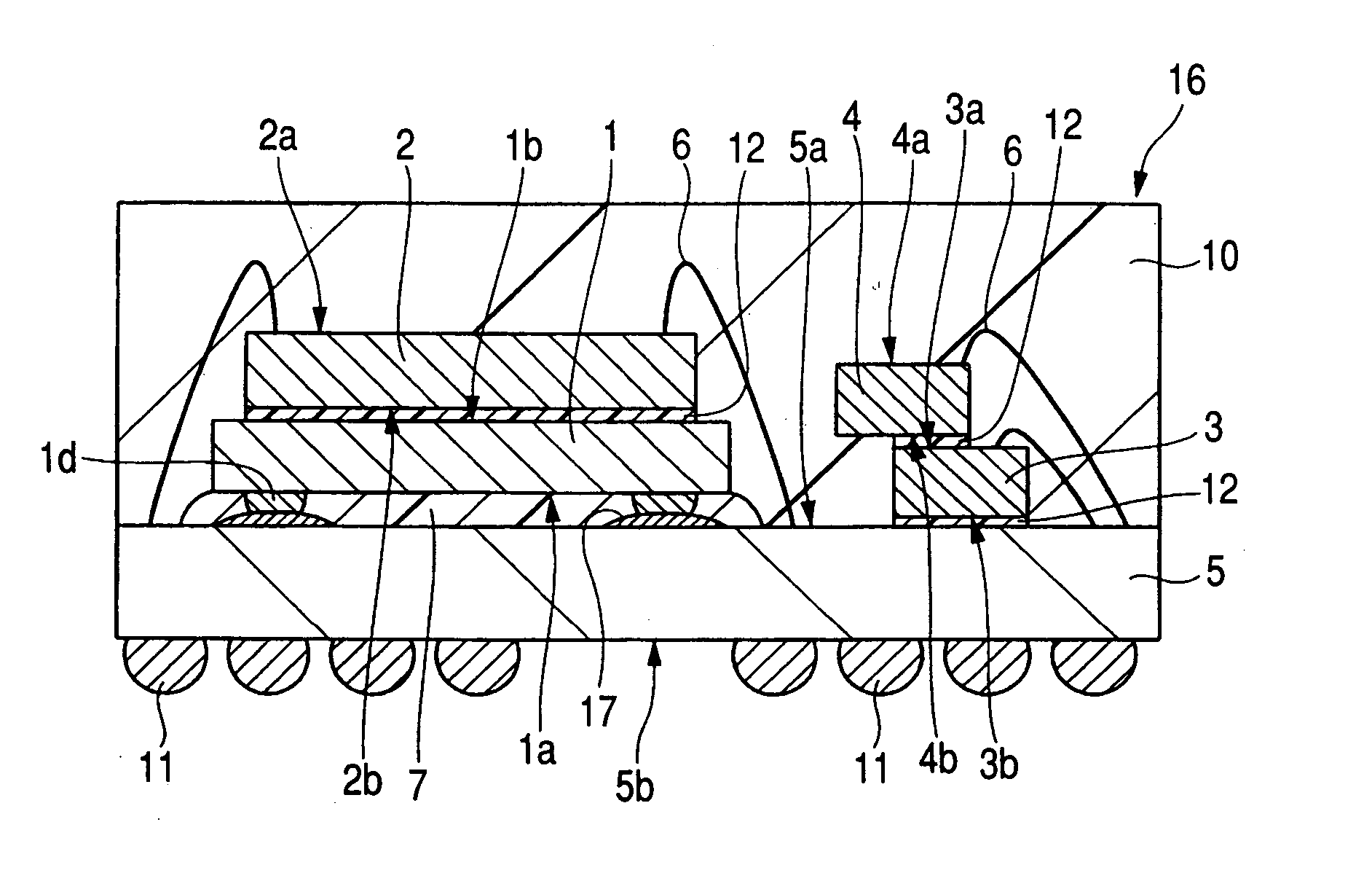
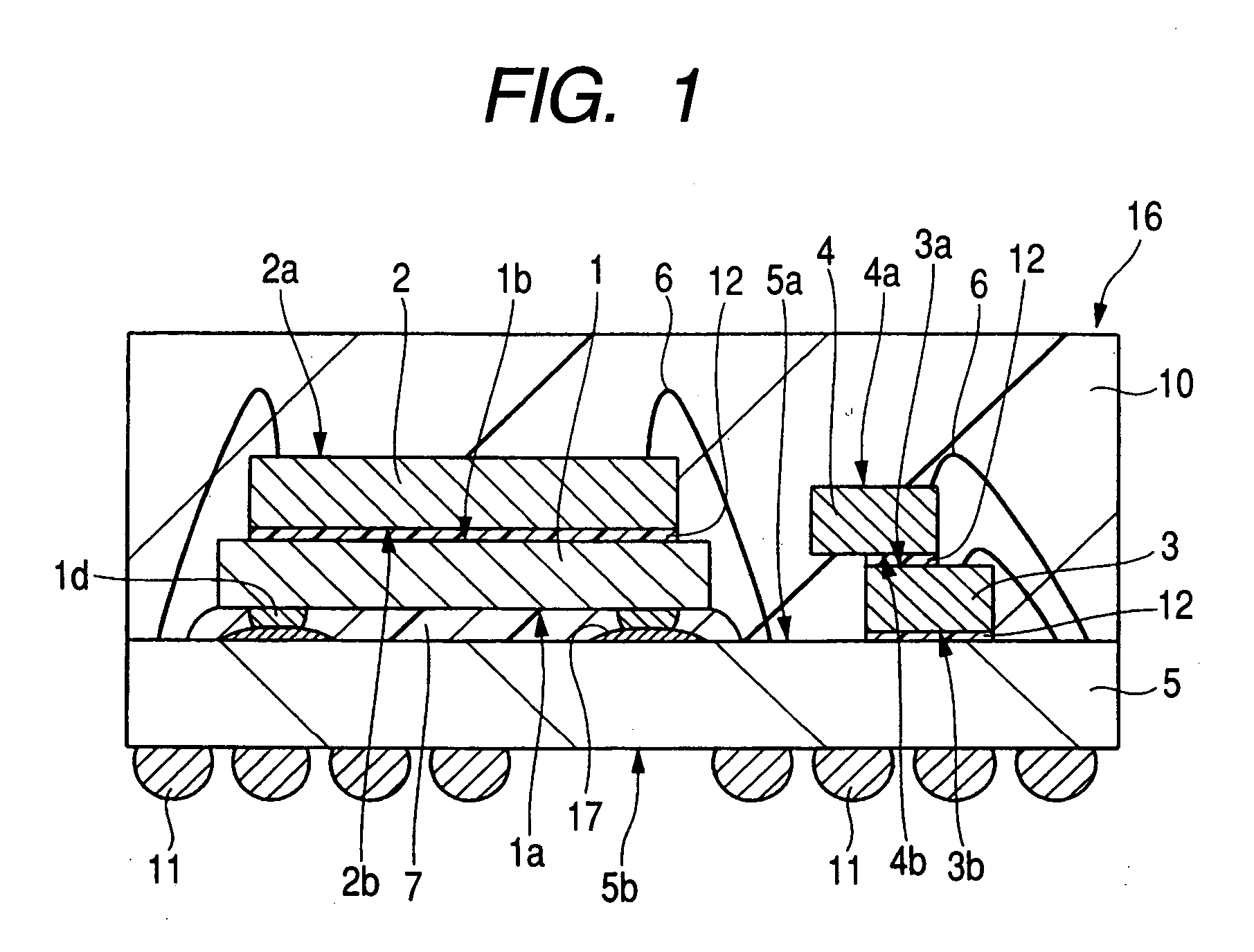
[0061] The semiconductor device of the embodiment shown in FIG. 1 has a structure in which a semiconductor chip is flip-chip bonded to a wiring substrate. In this embodiment, an SIP (System In Package) 16 having four semiconductor chips and which is sealed with a resin will be described as an example of the above-mentioned semiconductor device.
[0062] The SIP 16 comprises a first semiconductor chip 1 for control, a second semiconductor chip 2, a third semiconductor chip 3 and a fourth semiconductor chip 4, each having a memory circuit. The first semiconductor chip 1 of these semiconductor chips is flip-chip bonded to a packaging board 5, which serves as a wiring substrate, through projecting electrodes, and the second semiconductor chip 2 is formed over the first semiconductor chip 1. The third semiconductor chip 3 is mounted over the packaging board 5, and the fourth semiconductor chip 4 is mounted over the third semiconductor chip 3 in such a manner that their main surfaces 3a and...
PUM
 Abstract
Description
Claims
Application Information
 - R&D Engineer
- R&D Manager
- IP Professional
- Industry Leading Data Capabilities
- Powerful AI technology
- Patent DNA Extraction
Browse by: Latest US Patents, China's latest patents, Technical Efficacy Thesaurus, Application Domain, Technology Topic.
© 2024 PatSnap. All rights reserved.Legal|Privacy policy|Modern Slavery Act Transparency Statement|Sitemap