Dielectric resonator having a multilayer structure

a dielectric resonator and multi-layer technology, applied in the direction of waveguide devices, resonators, basic electric elements, etc., can solve the problems of increased manufacturing costs, difficult to miniaturize and difficulty in fabricating the dielectric resonant device to have a high q factor, so as to reduce the loss of dielectric resonators. , the effect of reducing the loss

Inactive Publication Date: 2005-06-30
POSTECH ACAD IND FOUND
View PDF3 Cites 24 Cited by
  • Summary
  • Abstract
  • Description
  • Claims
  • Application Information

AI Technical Summary

Benefits of technology

[0007] It is, therefore, an object of the present invention to provide a multi-layer dielectric resonant device, in which a multilayer dielectric resonator is implemented by stacking low dielectric constant layers and a high dielectric constant layer, and placing a metallic substrate in a center portion of the stacked dielectric layers, and a microstrip line is placed to be coupled to the multilayer dielectric resonator, so that a conductor loss of the device can be reduced, Q value of the device can be increased, and the device using the dielectric resonator can be fabricated with a high degree of integration.
[0008] In accordance with a preferred embodiment of the present invention, there is provided a multi-layer dielectric resonant device having a dielectric resonator and a microstrip line to be coupled to the dielectric resonator, the dielectric resonator including: a first dielectric layer having a first dielectric constant; a second dielectric layer having a second dielectric constant higher than the first dielectric constant, which is placed on the first dielectric layer; a third dielectric layer having a third dielectric constant lower than the second dielectric constant, which is placed on the second dielectric layer; a metallic substrate, which is placed in a center portion of the second dielectric layer, for reducing a conductor loss of the dielectric resonator; and a metallic plate for surrounding the first, second and third dielectric layers, thereby forming an outer wall of the dielectric resonator.
[0009] In accordance with another preferred embodiment of the present invention, there is provided a multi-layer dielectric resonant device having a dielectric resonator and a microstrip line to be coupled to the dielectric resonator, the dielectric resonator including: a first dielectric layer having a first dielectric constant; a second dielectric constant layer having a second dielectric constant, which is placed on the first dielectric layer and provided with a hole at a center portion thereof; a third dielectric layer having a third dielectric constant higher than the first and second dielectric constants, which is placed within the hole of the second dielectric layer and on the first dielectric layer; a fourth dielectric layer having a fourth dielectric constant lower than the third dielectric constant, which is placed on the second dielectric layer and the third dielectric layer; a metallic substrate, which is placed in a center portion of the second dielectric layer, for reducing conductor loss of the dielectric resonator; and a metallic plate for surrounding the first, second, third and fourth dielectric layers, thereby forming an outer wall of the dielectric resonator.

Problems solved by technology

However, the conventional dielectric resonant device has a problem in that it is difficult to fabricate the dielectric resonant device to have a high Q factor (quality factor) due to a conductor loss of the microstrip line 12 even though the dielectric resonator 14 has a high Q factor.
Furthermore, in the conventional dielectric resonant device, the dielectric resonator 14, which is separately manufactured, is attached to the dielectric layer 10, so that a problem arises in that it is difficult to miniaturize the dielectric resonant device, and the manufacturing costs thereof are increased.

Method used


Image

  • Dielectric resonator having a multilayer structure
  • Dielectric resonator having a multilayer structure
  • Dielectric resonator having a multilayer structure

Examples


first embodiment

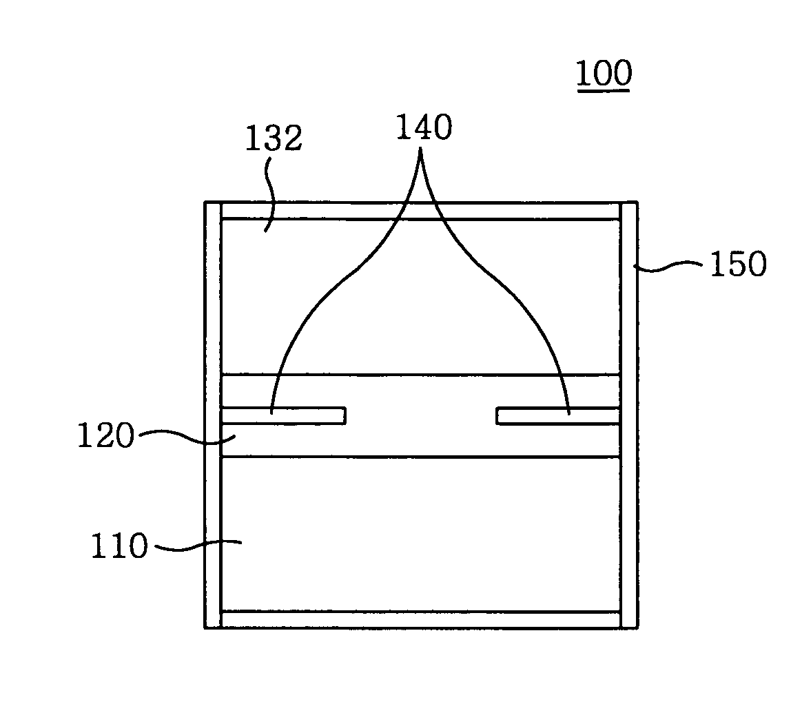
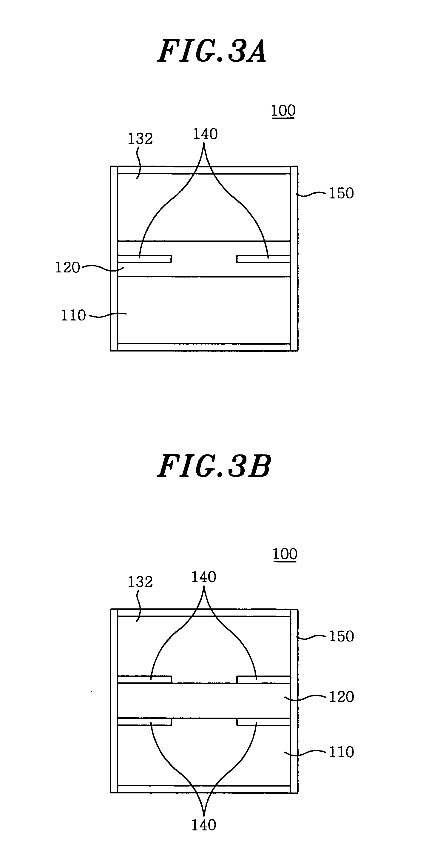
[0027]FIG. 3A shows a cross-sectional view of a multi-layer dielectric resonator 100 in accordance with the present invention. The multilayer dielectric resonator 100 includes a first dielectric layer 110 having a first dielectric constant, a second dielectric layer 120 having a second dielectric constant higher than the first dielectric constant, which is placed on the first dielectric layer 110, a third dielectric layer 132 having a third dielectric constant lower than the second dielectric constant, which is placed on the second dielectric layer 120, a metallic substrate 140, which is placed in a center portion of the second dielectric layer 120, to reduce a conductor loss of the dielectric resonator 100, and a metallic plate 150 for forming an outer wall of the dielectric resonator 100 and blocks loss attributable to an RF wave radiation of a microstrip line to be coupled to the dielectric resonator 100.

[0028] In this embodiment, the first and third dielectric layers 110 and 132...

second embodiment

[0038]FIG. 8 exhibits a dielectric resonator 100 in accordance with the present invention. Referring to FIG. 8, the dielectric resonator 100 includes a first dielectric layer 110 having a first dielectric constant, a third dielectric layer 132 having a third dielectric constant, which is placed on the first dielectric layer 110, a second dielectric layer 120 having a second dielectric constant higher than the first and third dielectric constant, which is placed within a center hole of the third dielectric layer 132 and on the first dielectric layer 110, a fourth dielectric layer 133 having a fourth dielectric constant lower than the second dielectric constant, which is placed on the third dielectric layer 132 and the second dielectric layer 120, a metallic substrate 140 that is placed in the center portion of the third dielectric layer 132 to reduce a conductor loss of the dielectric resonator 100, and a metallic plate 150 that constitutes an outer wall of the dielectric resonator 1...


PUM


Abstract

A multi-layer dielectric resonant device has a dielectric resonator and a microstrip line to be coupled to the dielectric resonator. The dielectric resonator includes a first dielectric layer, a second dielectric layer, a third dielectric layer, a metallic substrate and a metallic plate. The second dielectric layer is placed on the first dielectric layer and has a dielectric constant higher than that of the first dielectric layer. The third dielectric layer is placed on the second dielectric layer and has a dielectric constant lower than that of the second dielectric layer. The metallic substrate is placed in the center portion of the second dielectric constant layer to reduce the conductor loss of the dielectric resonator. The metallic plate constitutes the outer wall of the dielectric resonator.

Description

FIELD OF THE INVENTION [0001] The present invention relates to a multi-layer dielectric device; and, more particularly, to a multi-layer dielectric resonant device, in which a multilayer dielectric resonator is implemented by stacking low dielectric constant layers and a high dielectric constant layer, and placing a metallic substrate in a center portion of the stacked dielectric layers, and a microstrip line is placed to be coupled to the multilayer dielectric resonator, so that a conductor loss of the device can be reduced and Q factor of the device can be increased. BACKGROUND OF THE INVENTION [0002] In general, with the increase in demand for exchanges of information via wireless communications, needs for communications systems using microwaves are increasing. Devices used in a wireless communications field tend to have a smaller size and a higher capacity. Furthermore, working frequencies thereof are changed to a high frequency band, and thus the GHz frequency band is being uti...

Claims


Application Information

Patent Timeline
Patent Type & Authority Applications(United States)
IPC IPC(8): H01P1/20H01P7/10H01P1/203
CPCH01P7/10H01P1/203
Inventor KIM, BUMMANYIM, JOUNG HYUN
Owner POSTECH ACAD IND FOUND
Why Eureka
Try Eureka