Image reading apparatus, image recording medium and image forming apparatus
a reading apparatus and image recording technology, applied in the direction of instruments, diffusion transfer processes, optics, etc., can solve the problems of large amount of light lost at the time of image reading, difficult for photoelectric conversion elements to obtain sufficient light, and output signals with a high sn-ratio, etc., to achieve satisfactory image, wide dynamic range, and wide dynamic range
- Summary
- Abstract
- Description
- Claims
- Application Information
AI Technical Summary
Benefits of technology
Problems solved by technology
Method used
Image
Examples
first embodiment
[0075] (First Embodiment)
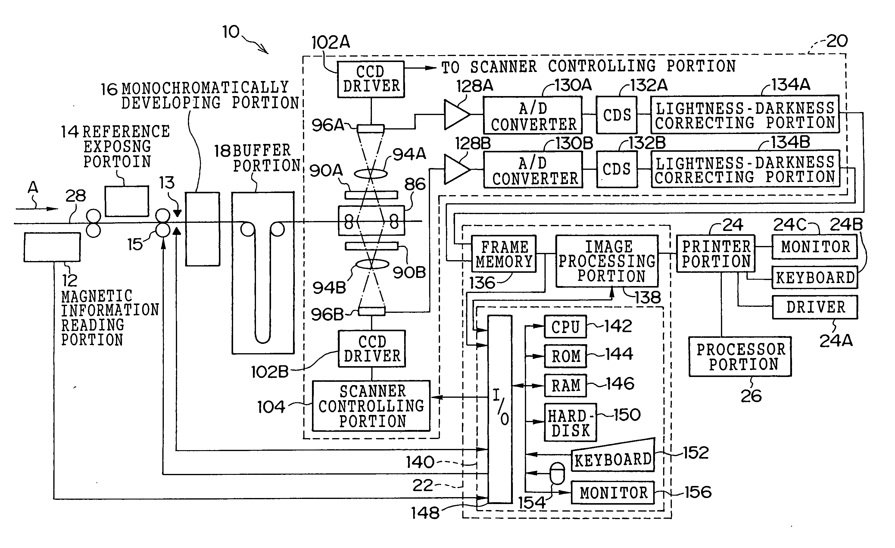
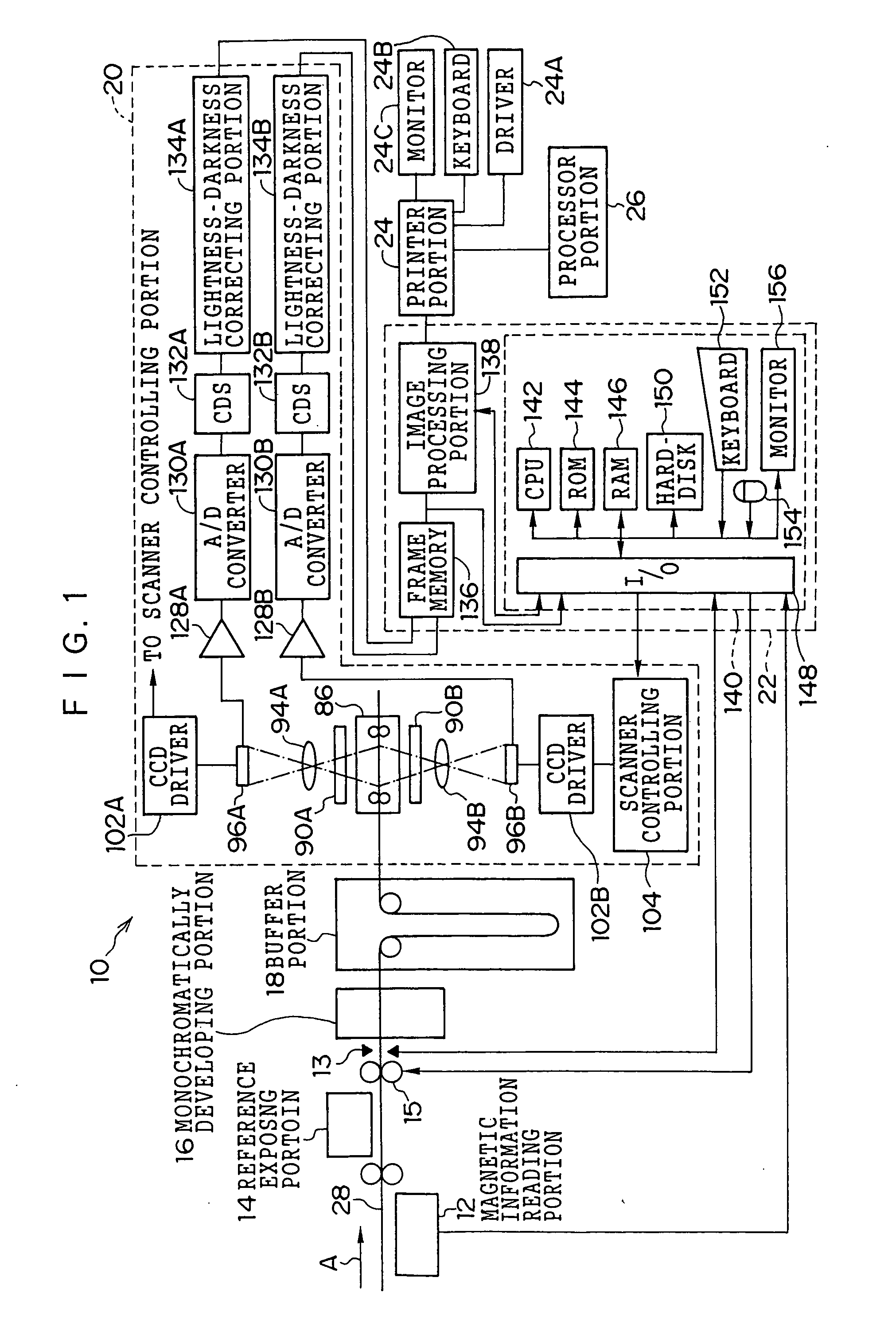
[0076]FIG. 1 shows an overall structure of an image processing system 10. As shown in FIG. 1, the image processing system 10 consists of a magnetic information reading portion 12, a reference exposing portion 14, a perforation detecting sensor 13 which is used when an APS film is being read, a monochromatic developing portion 16, a buffer portion 18, a film scanner 20, an image processing device 22, a printer portion 24 and a processor portion 26. The perforation detecting sensor 13 is structured so that a light emitting element and a light receiving element are disposed opposite to each other.
[0077] The image processing system 10 reads film images (silver images) recorded on a color photographic film such as a negative film or a reversal film (positive film), performs an image processing, and prints the processed images on photographic printing papers. The image processing system 10 can process film images on, for example, the following types of photograph...
second embodiment
[0165] (Second Embodiment)
[0166] In the first embodiment, the illuminating units 90A and 90B emit light having the same wavelength (IR light having a central wavelength of about 950 nm). However, the illuminating units 90A and 90B may emit light having different wavelengths,(e.g., 850 nm and 1,310 nm). In this case, reflected light and transmitted light can be simultaneously detected. Namely, as shown in FIG. 21, a half mirror 91A is disposed between the focusing lens 94A and an area corresponding to an area in which the area CCD 96A is disposed in FIG. 11, and in place of the area CCD 96A which has sensitivity for IR light having a central wavelength of about 950 nm, area CCDs 96A1 and 96A2, which have sensitivity for light of different wavelengths, are respectively disposed in directions in which light is branched by the half mirror 91A. Similarly, a half mirror 91B is disposed between the focusing lens 94B and an area corresponding to an area in which the area CCD 96B is disposed...
PUM
| Property | Measurement | Unit |
|---|---|---|
| central wavelength | aaaaa | aaaaa |
| light transmittance | aaaaa | aaaaa |
| time | aaaaa | aaaaa |
Abstract
Description
Claims
Application Information


