Horizontal chalcogenide element defined by a pad for use in solid-state memories

a technology of chalcogenide elements and solid-state memories, which is applied in semiconductor devices, digital storage, instruments, etc., can solve the problems of reducing the current/power requirements of the resulting chalcogenide memory devices, and achieves the effects of effective depositing chalcogenide into ultra-small pores, good thickness control, and relative ease of fabrication

Active Publication Date: 2005-07-07
MACRONIX INT CO LTD
View PDF12 Cites 115 Cited by
  • Summary
  • Abstract
  • Description
  • Claims
  • Application Information

AI Technical Summary

Benefits of technology

[0009] The present invention discloses a chalcogenide element structure and two innovative methods in the formation of chalcogenide phase change memories. The cross-sectional areas of the chalcogenide elements produced by these methods are relatively small, resulting in dramatically decreased current / power requirements of the resulting chalcogenide memory devices.
[0013] There need not be etched pores in either method, thus removing photolithography as a limit to the cross-sectional areas of the chalcogenide elements. The problem of effectively depositing chalcogenide into ultra small pores is also eliminated. The chalcogenide element can be fabricated with relative ease since there is no need to place material into small pores.
[0014] In accordance with another aspect of the present invention, the cross-sectional area of each chalcogenide element is defined by the thickness of the first layer, the thickness of the second layer, and the etch back process on the second layer. With good control of the thickness for each of the two films, the cross-sectional area can be made relatively very small. The smaller area reduces the current required in the chalcogenide phase change memory. The cross-sectional area of the chalcogenide element is relatively easy to scale down since the scaling limit of thin film and etch back processes is less than 50 Å in 0.25-μm technology. For example, if the first layer thickness is 500 Å and the second layer thickness is 200 Å, which are relatively easy to fabricate by 0.25-μm processes, the cross-sectional area will be less than 105 Å2. This dimension corresponds to a contact pore with a diameter of 0.036 μm, which is cumbersome to nearly impossible to fabricate today using conventional methods. Any feature or combination of features described herein are included within the scope of the present invention provided that the features included in any such combination are not mutually inconsistent as will be apparent from the context, this specification, and the knowledge of one of ordinary skill in the art. For purposes of summarizing the present invention, certain aspects, advantages and novel features of the present invention have been described herein. Of course, it is to be understood that not necessarily all such aspects, advantages or features will be embodied in any particular embodiment of the present invention. Additional advantages and aspects of the present invention are apparent in the following detailed description and claims.

Problems solved by technology

The cross-sectional areas of the chalcogenide elements produced by these methods are relatively small, resulting in dramatically decreased current / power requirements of the resulting chalcogenide memory devices.

Method used


Image

  • Horizontal chalcogenide element defined by a pad for use in solid-state memories
  • Horizontal chalcogenide element defined by a pad for use in solid-state memories
  • Horizontal chalcogenide element defined by a pad for use in solid-state memories

Examples


Embodiment Construction

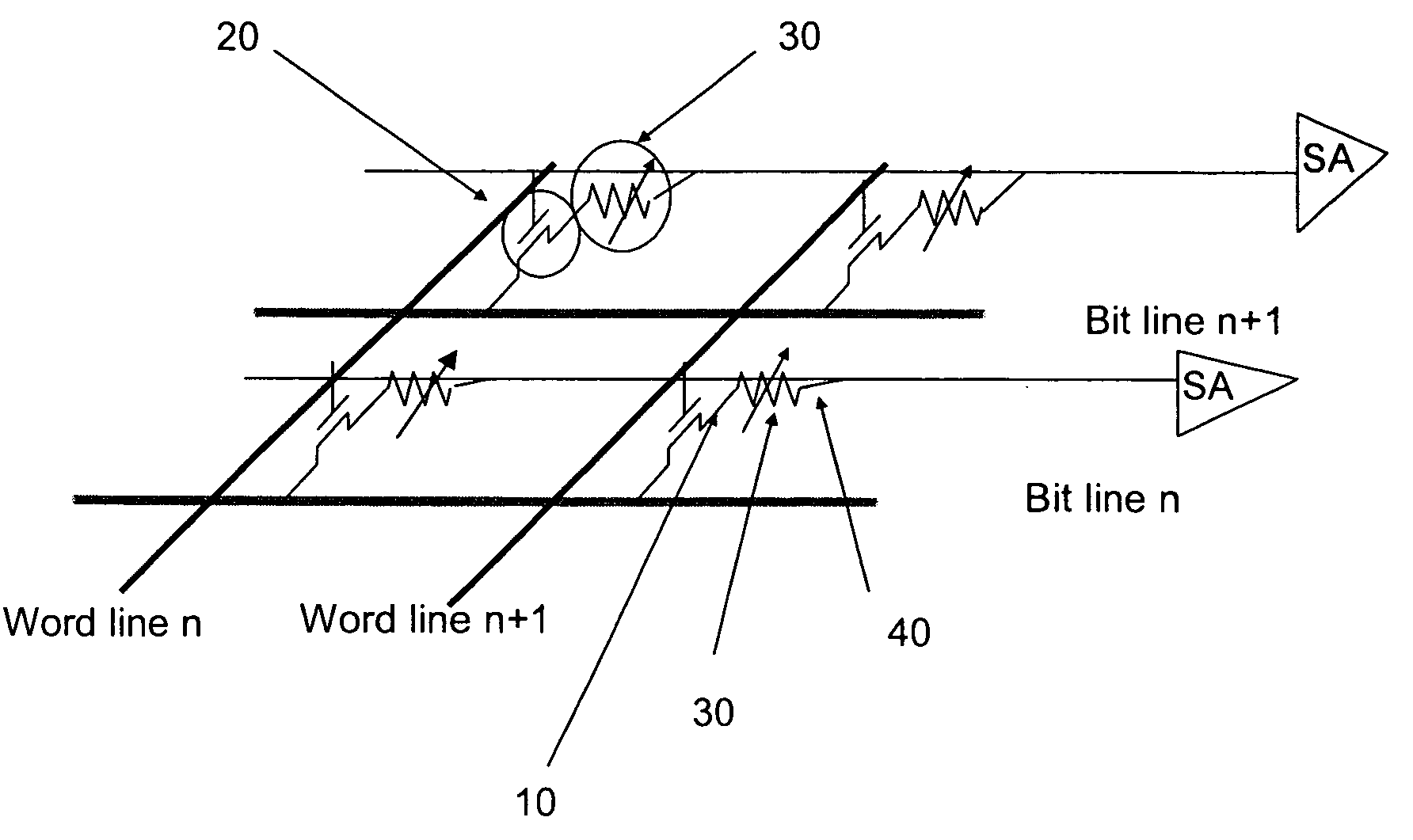
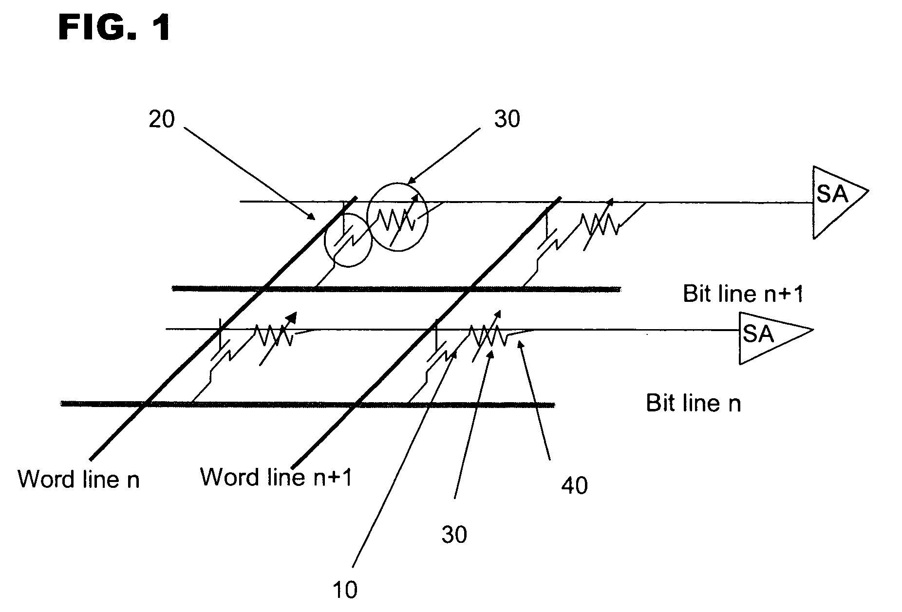
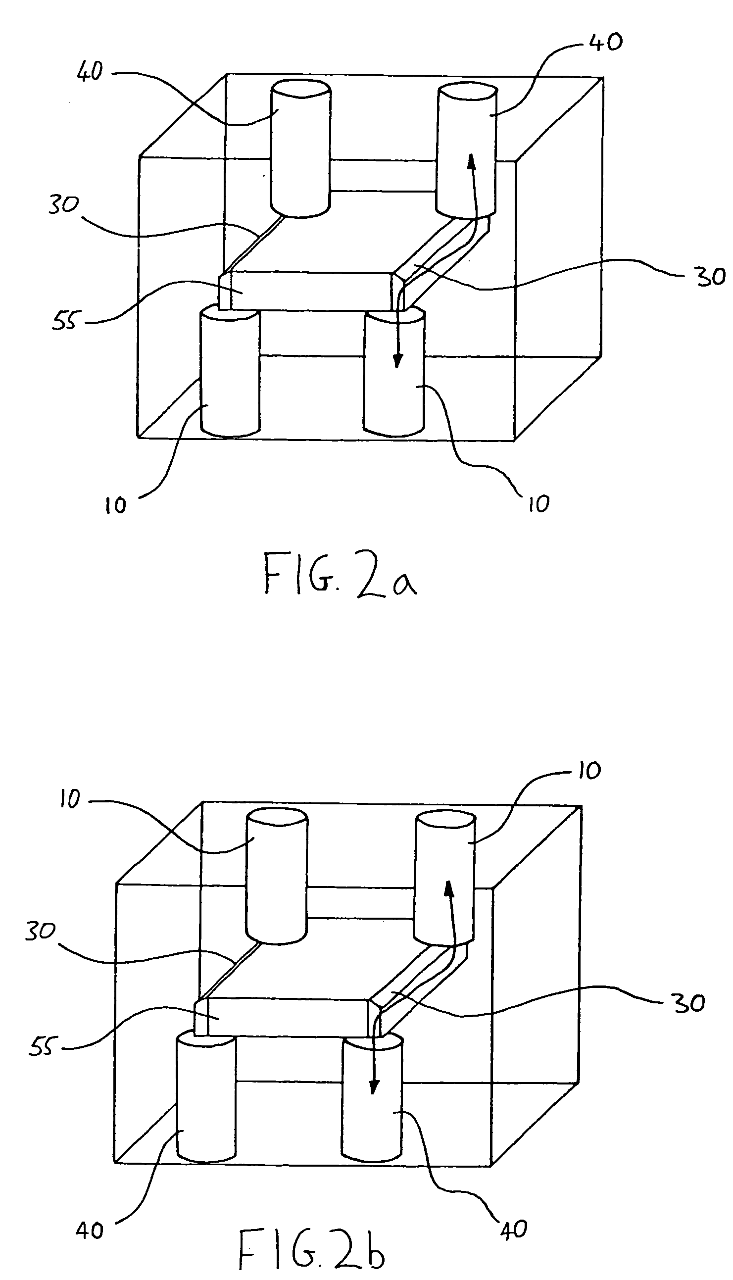
[0036] Two methods of fabricating elements are presented that provide element cross-sectional areas which may be smaller than that presently provided using conventional and some modified photolithographic methods. In particular, the illustrated embodiments disclosed herein exemplify methods in accordance with the present invention of fabricating elements that rely upon pads to define minimum heights of the elements and rely upon thicknesses of element comprising films (disposed over the pads) to define minimum widths of the elements. In either manner, phase change elements having minimum heights of about 20 Å and minimum widths of about 20 Å can be obtained.

[0037] Reference will now be made in detail to the presently preferred embodiments of the invention, examples of which are illustrated in the accompanying drawings. Wherever possible the same or similar reference numbers are used in the drawings and the description to refer to the same or like parts. It should be noted that the ...


PUM


Abstract

A process for fabricating phase-change elements having ultra small cross-sectional areas for use in phase change memory cells specifically and in semiconductor devices generally in which pads are implemented to create horizontally aligned phase change elements is disclosed. The elements thus defined may be used within chalcogenide memory cells or other semiconductor devices.

Description

BACKGROUND OF THE INVENTION [0001] 1. Field of the Invention [0002] The present invention relates generally to semiconductor fabrication methods and, more particularly, to the fabrication of horizontal chalcogenide memory devices. [0003] 2. Description of Related Art [0004] Electrically writable and erasable phase change materials have traditionally been used for memory devices. Chalcogenide materials can be electrically switched between two structural states of generally crystalline and generally amorphous local order. The generally crystalline state is a phase in which the material's atoms and / or electrons form a repeatable lattice structure, whereas the atoms and / or electrons of the generally amorphous state are randomly distributed. The structural state can also be switched among a range of detectable structural states of local order between the extremes of completely crystalline and completely amorphous states. [0005] The currently favored chalcogenide materials that are used f...

Claims


Application Information

Patent Timeline
Patent Type & Authority Applications(United States)
IPC IPC(8): G11C16/02H01L27/24H01L29/00H01L45/00
CPCG11C13/0004H01L27/2463H01L45/1691H01L45/1226H01L45/144H01L45/06H10B63/80H10N70/823H10N70/231H10N70/068H10N70/8828
Inventor CHEN, YI-CHOULUNG, HSIANG-LANLIU, RUICHEN
Owner MACRONIX INT CO LTD
Why Eureka
Try Eureka