Stacked light emitting diode

a light-emitting diode and stacking technology, which is applied in the direction of discharge tube luminescnet screens, discharge tube/lamp details, electric discharge lamps, etc., can solve the problems of unfulfilled trends of light-emitting chips, small volume and light weight required by modern techniques, and insufficient intensity of light-emitting chips, etc., to achieve easy manufacturing and assembly processes, high light intensity effects, and reduced occupied area

Inactive Publication Date: 2005-07-07
LIGHTOP TECH
View PDF3 Cites 13 Cited by
  • Summary
  • Abstract
  • Description
  • Claims
  • Application Information

AI Technical Summary

Benefits of technology

[0009] The primary object of the invention is to provide a stacked light emitting diode comprising at least two light emitting chips stacked at a stand or a circuit board, thereby accomplishing multicolor variations and high light intensity effects.
[0010] The secondary object of the invention is to provide a stacked light emitting diode having minimized light emitting chips for reducing an occupied area, thereby facilitating manufacturing and assembly processes of the structure.
[0011] The other object of the invention is to provide a stacked light emitting diode, in that circuits are connected in series or in parallel, thereby expanding product application ranges and efficacies.
[0012] T...

Problems solved by technology

In addition, during illumination, energies released by the light emitting chips are not totally focused, so that intensity of the light emitting chips appears somewhat inadequate.
Furthermore, an occupied area is rather large that trends as being light in weight and small in volume required by modern techniques are left unfulfilled.
Also, this prior structure comprising illuminating the chips a1 and a2 hardly offers maximum industrial practicability for that...

Method used


Image

  • Stacked light emitting diode
  • Stacked light emitting diode
  • Stacked light emitting diode

Examples


Embodiment Construction

[0020] To better understand structural characteristics and functions of the invention, detailed descriptions shall be given with the accompanying drawings hereunder.

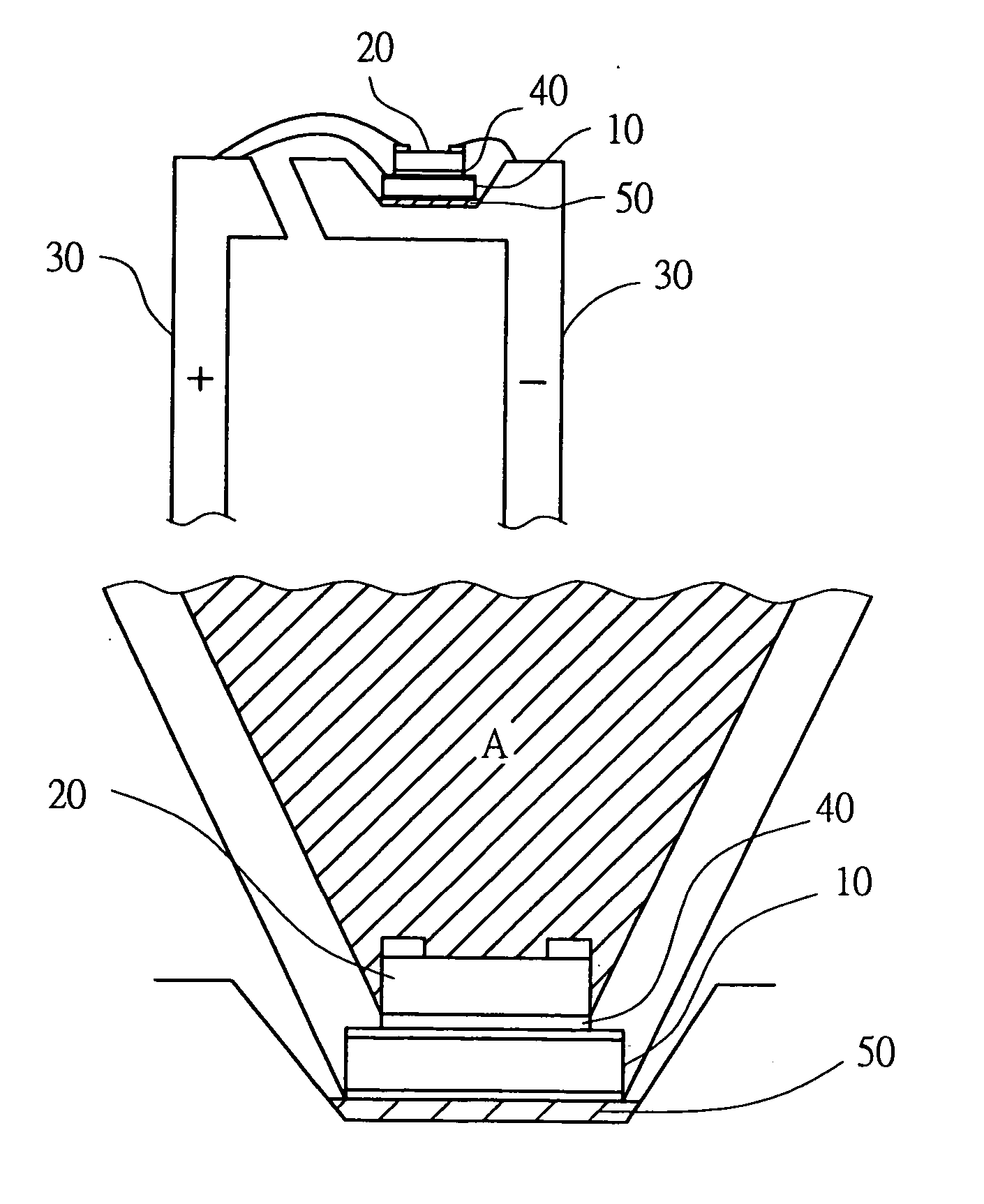
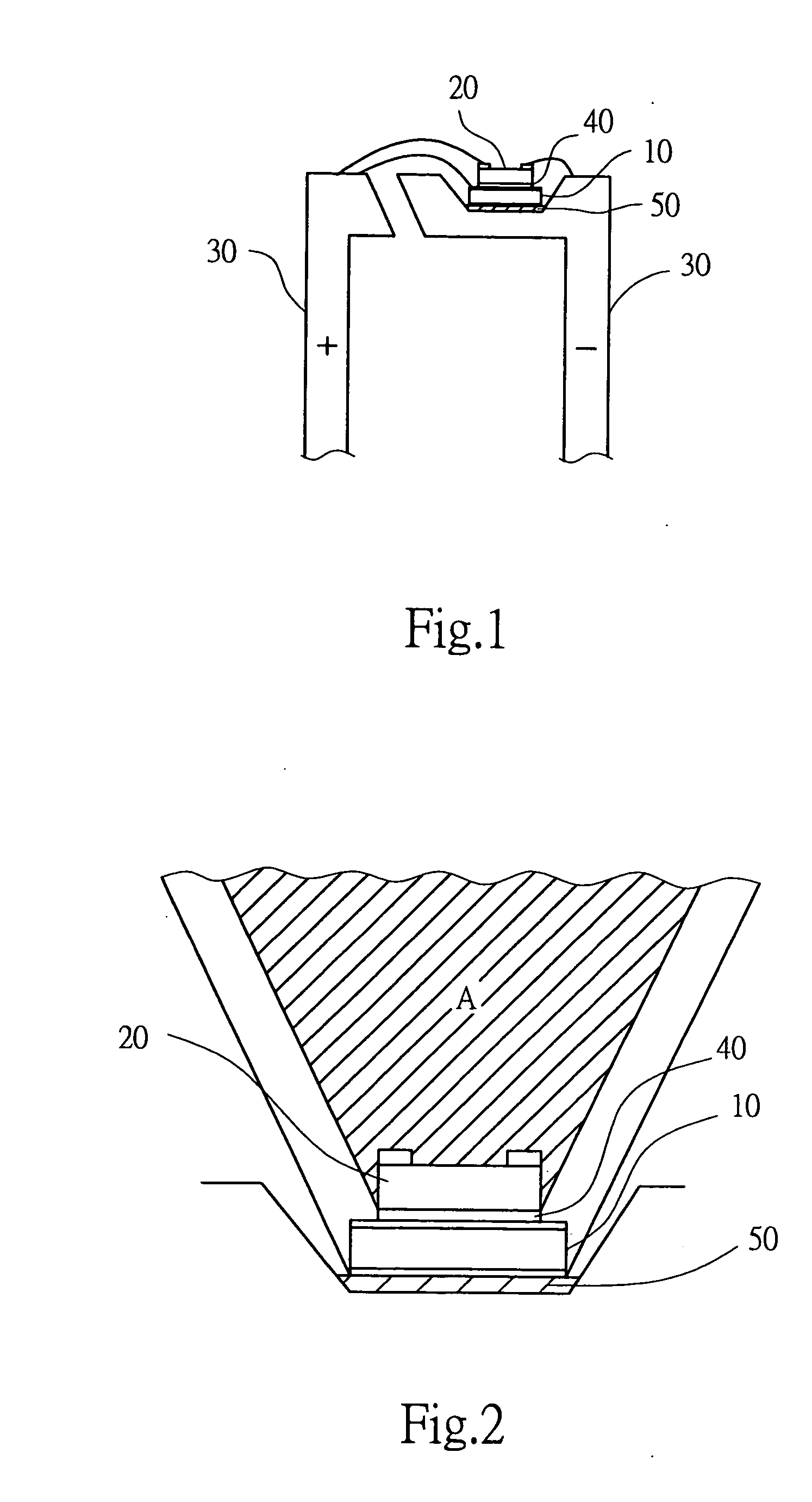
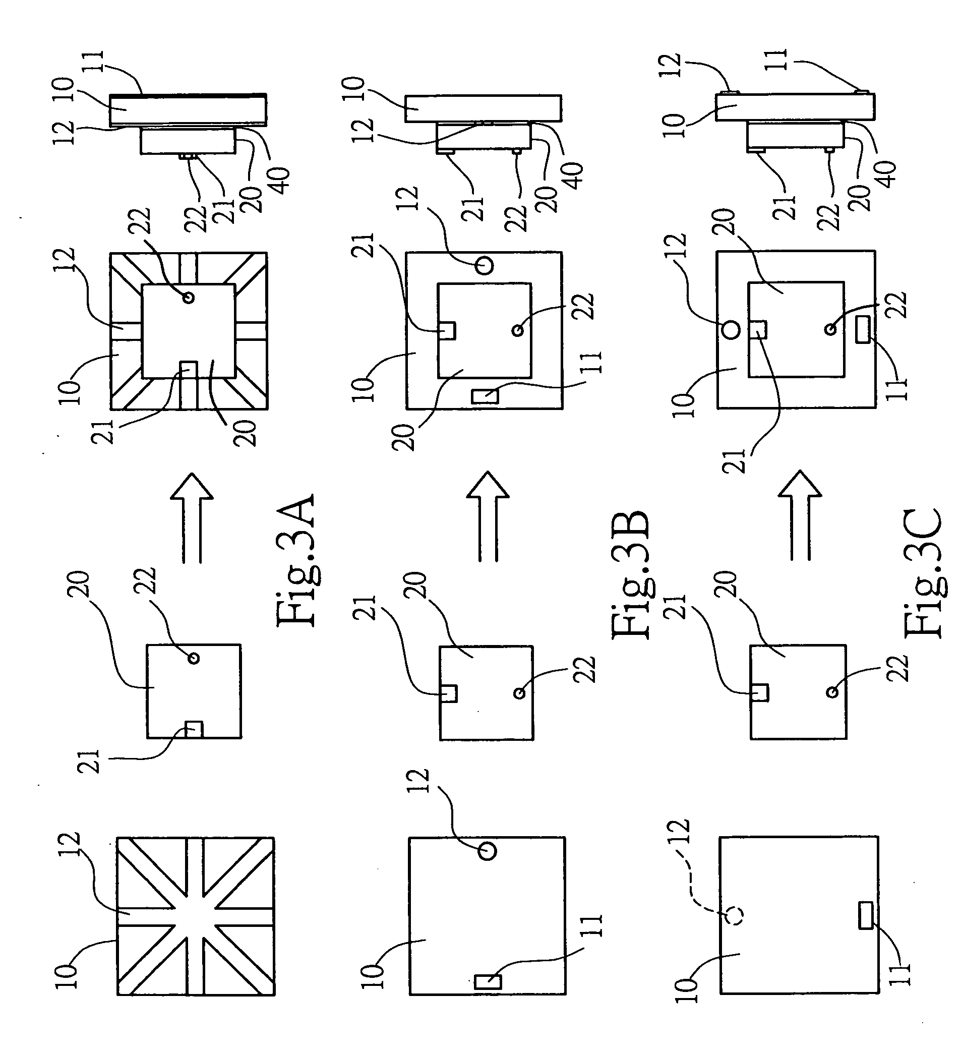
[0021] With reference of FIGS. 1 and 2, a stacked light emitting diode according to the invention comprises a light emitting chip 10 fixed at a circuit board or a substrate and stacked with one or more than one light emitting chip 20 thereon. The light emitting chips 10 and 20 have different illumination wavelengths (colors). In conjunction with a CIE hue chart, blended light effects can be achieved by the light emitting chips 10 and 20 having different wavelengths. The invention is characterized that, a lower-layer light emitting chip 10 is a light-transmissive or opaque chip, a second or a third light emitting chip 20 stacked on the thereon is necessarily a light-transmissive chip, and between the stacked chips is a light-transmissive insulating material 40 for fixing the chips.

[0022] When putting the aforesaid struc...


PUM


Abstract

A stacked light emitting diode structure includes a light emitting chip fixed at a stand and stacked thereon with one or more than one smaller light emitting chip. Wherein, the light emitting chips have different illumination wavelengths. The invention is characterized that, a lower-layer light emitting chip is a light-transmissive or opaque chip, a second or a third light emitting chip stacked thereon is necessarily a light-transmissive chip, and between the stacked chips is a light-transmissive insulating material for fixing the chips. When putting the aforesaid structure to use, efficacies as better blended light effects and intensity as well as a reduced occupied area are obtained.

Description

BACKGROUND OF THE INVENTION [0001] (a) Field of the Invention [0002] The invention relates to a stacked light emitting diode, and more particularly, to a light emitting diode capable of emitting multiple colors and formed by two light emitting chips having different wavelengths (illumination colors), with circuits thereof connected in series or in parallel, thereby accomplishing variations of multiple colors and increasing intensity as well as minimizing an occupied area of the chips. [0003] (b) Description of the Prior Art [0004] Referring to FIG. 5A showing a prior multicolor light illuminating diode, two (or three) light emitting diodes a1 and a2 are individually fixed to a stand b (or a circuit board). Electrodes of the light emitting chips a1 and a2 are generally arranged at lower and upper surfaces of the chips. The light emitting chips a1 and a2 have lower surfaces thereof connected to the stand b (or the circuit board) using electrically conductive glue c, and electrodes at ...

Claims


Application Information

Patent Timeline
IPC IPC(8): H01J1/62H01L25/075
CPCH01L25/0756H01L2924/3025H01L2224/45144H01L2224/45124H01L2224/32145H01L2224/49113H01L2224/48257H01L2224/48247H01L2224/32245H01L2224/73265H01L2924/00
Inventor HO, YING-MING
Owner LIGHTOP TECH
Why Eureka
Try Eureka