Circuit board assembly and method of attaching a chip to a circuit board

a circuit board and circuit board technology, applied in the direction of individual energised antenna arrays, semiconductor/solid-state device details, particular array feeding systems, etc., can solve the problems of increasing the amount of board area used, increasing the weight and bulk of the assembly, and contributing to the time and cost of manufactur

Active Publication Date: 2005-07-14
RAYTHEON CO
View PDF7 Cites 68 Cited by
  • Summary
  • Abstract
  • Description
  • Claims
  • Application Information

AI Technical Summary

Problems solved by technology

Such packages and connecting structures contribute to increased weight and bulk of the assembly and increase the amount of board area used.
Assembly may also require numerous steps which contribute to the time and cost of manufacture.

Method used


Image

  • Circuit board assembly and method of attaching a chip to a circuit board
  • Circuit board assembly and method of attaching a chip to a circuit board
  • Circuit board assembly and method of attaching a chip to a circuit board

Examples


Embodiment Construction

[0014] In the following detailed description and in the several figures of the drawing, like elements are identified with like reference numerals.

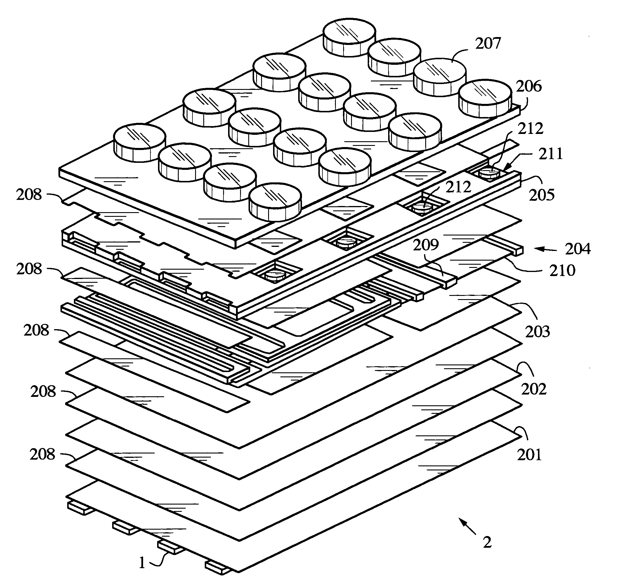
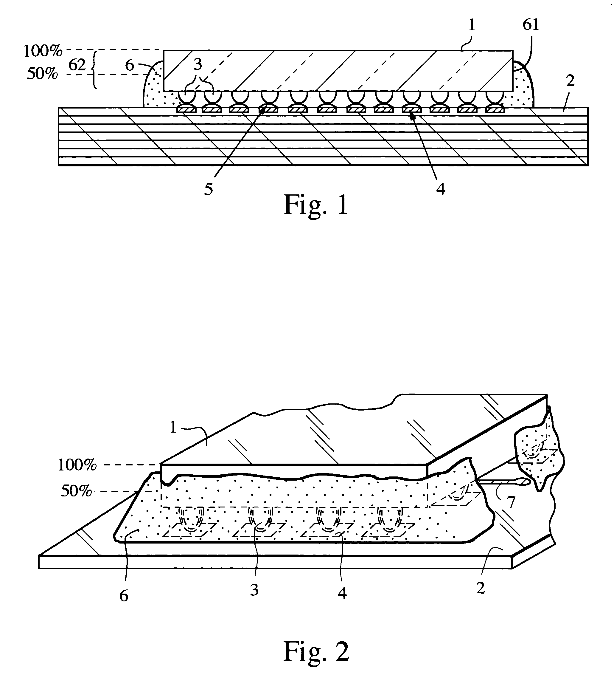
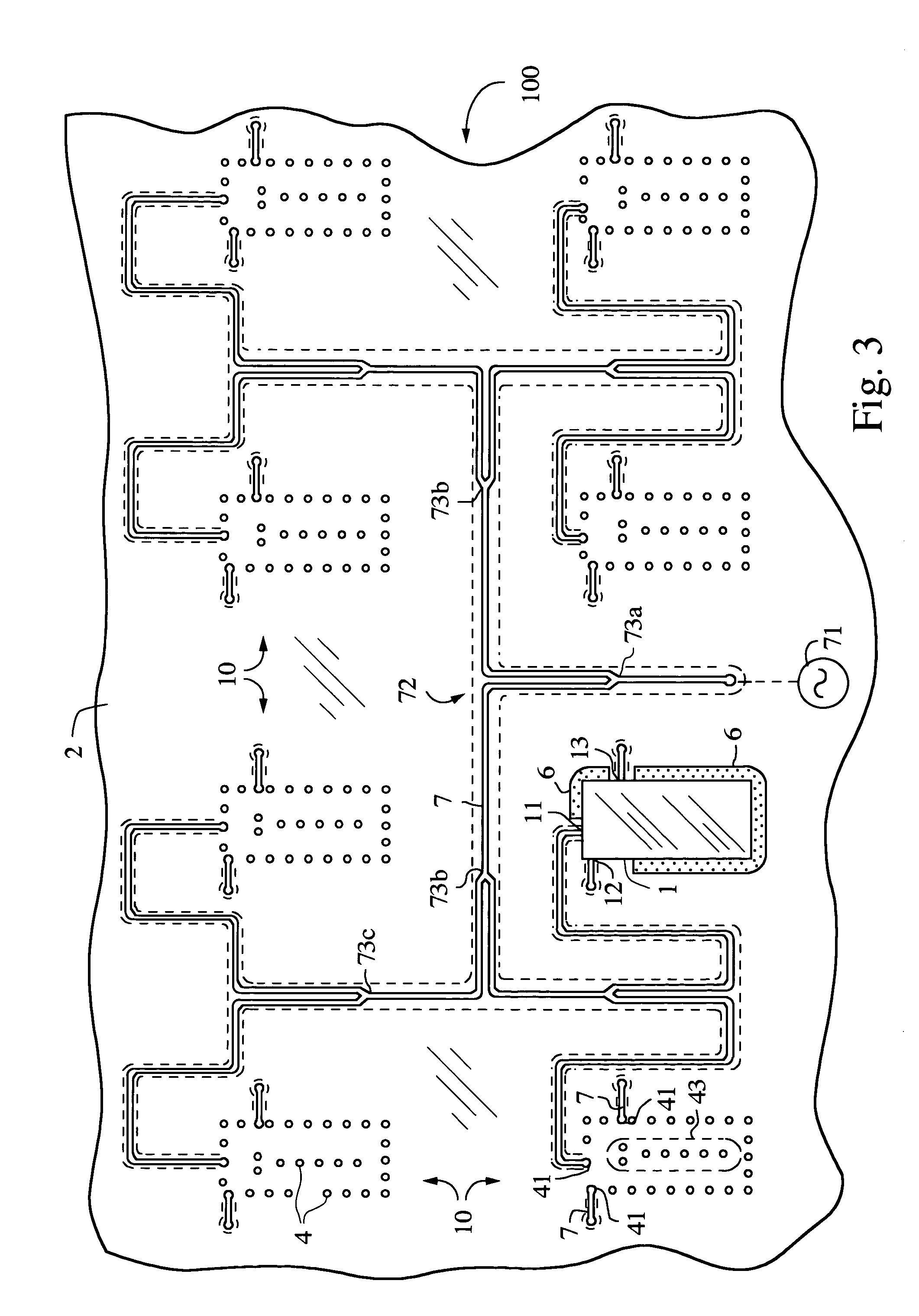
[0015]FIG. 1 illustrates an exemplary embodiment of a chip 1 connected to a circuit board 2. In the exemplary embodiment FIG. 1, the chip 1 is a transmit / receive (T / R) device chip 1 connected to a circuit board 2. In the embodiment illustrated in FIG. 1, the circuit board 2 is a multi-layer antenna panel circuit assembly. The multi-layer antenna panel circuit assembly may be flexible or rigid. In alternate embodiments, the chip 1 could be a receive chip or any other chip suitable for attaching to a circuit board. The circuit board could be any circuit board suitable for attaching chips. The circuit board 2 is a medium for distributing power, RF, and digital signals. The RF signals may be distributed to an antenna array which could be on the circuit board or attached to the circuit board.

[0016] The T / R chip is a “flip chip” with connectin...


PUM


Abstract

An antenna array is assembled by direct attaching a flip chip transmit / receive (T / R) module to an antenna circuit board. A fillet bond is applied to the circuit board and the flip chip T / R module around at least a portion of the periphery of the flip chip T / R module.

Description

BACKGROUND OF THE DISCLOSURE [0001] Chips can be attached to a circuit board. For example, antenna arrays can be assembled using packaged transmission / receive (T / R) modules. Packaged module assemblies may be brick array or coplanar tile arrays. Such packaged assemblies may include fasteners, interconnect structures and connectors, including, for example, coaxial cable, “fuzz” buttons, ribbon and / or wire bonds. Such packages and connecting structures contribute to increased weight and bulk of the assembly and increase the amount of board area used. Assembly may also require numerous steps which contribute to the time and cost of manufacture. BRIEF SUMMARY [0002] An antenna array is assembled by a method which includes direct attaching a flip chip transmit / receive (T / R) module to an antenna circuit board. A fillet bond is applied to the circuit board and the flip chip T / R module around at least a portion of the periphery of the flip chip T / R module.BRIEF DESCRIPTION OF THE DRAWINGS [0...

Claims


Application Information

Patent Timeline
Patent Type & Authority Applications(United States)
IPC IPC(8): H01Q21/00
CPCH01Q21/0025H01Q21/0087H01L2224/73204H01L2924/07811H01L2924/1305H01L2924/00H01Q21/00H05K3/30H01Q23/00
Inventor HAUHE, MARK S.ROLSTON, KEVIN C.QUAN, CLIFTONFENGER, HAROLD S.WONG, TSE E.
Owner RAYTHEON CO
Why Eureka
Try Eureka