Electronic part test apparatus

a technology of electronic parts and test apparatus, applied in the direction of measurement devices, semiconductor/solid-state device testing/measurement, instruments, etc., can solve the problems of reducing difficult to move at a high speed, and affecting the test effect, so as to reduce the weight of the contact arm

Inactive Publication Date: 2005-07-14
ADVANTEST CORP
View PDF14 Cites 34 Cited by
  • Summary
  • Abstract
  • Description
  • Claims
  • Application Information

AI Technical Summary

Benefits of technology

[0011] As a result that the first contact arm comprises a holding side contact arm, a lock-and-free means and a fixing side contact arm, the lock-and-free means is provided between the holding side contact arm and the fixing side contact arm, and the lock-and-free means restrains or releases restriction of a planar movement of the holding si

Problems solved by technology

However, a contact arm configured as above has a relatively heavy weight and it is hard to move at a high speed.
This disadvantage becomes particularly noticeable when the number of contact arms increases along with an increase of a simultaneo

Method used


Image

  • Electronic part test apparatus
  • Electronic part test apparatus
  • Electronic part test apparatus

Examples


first embodiment

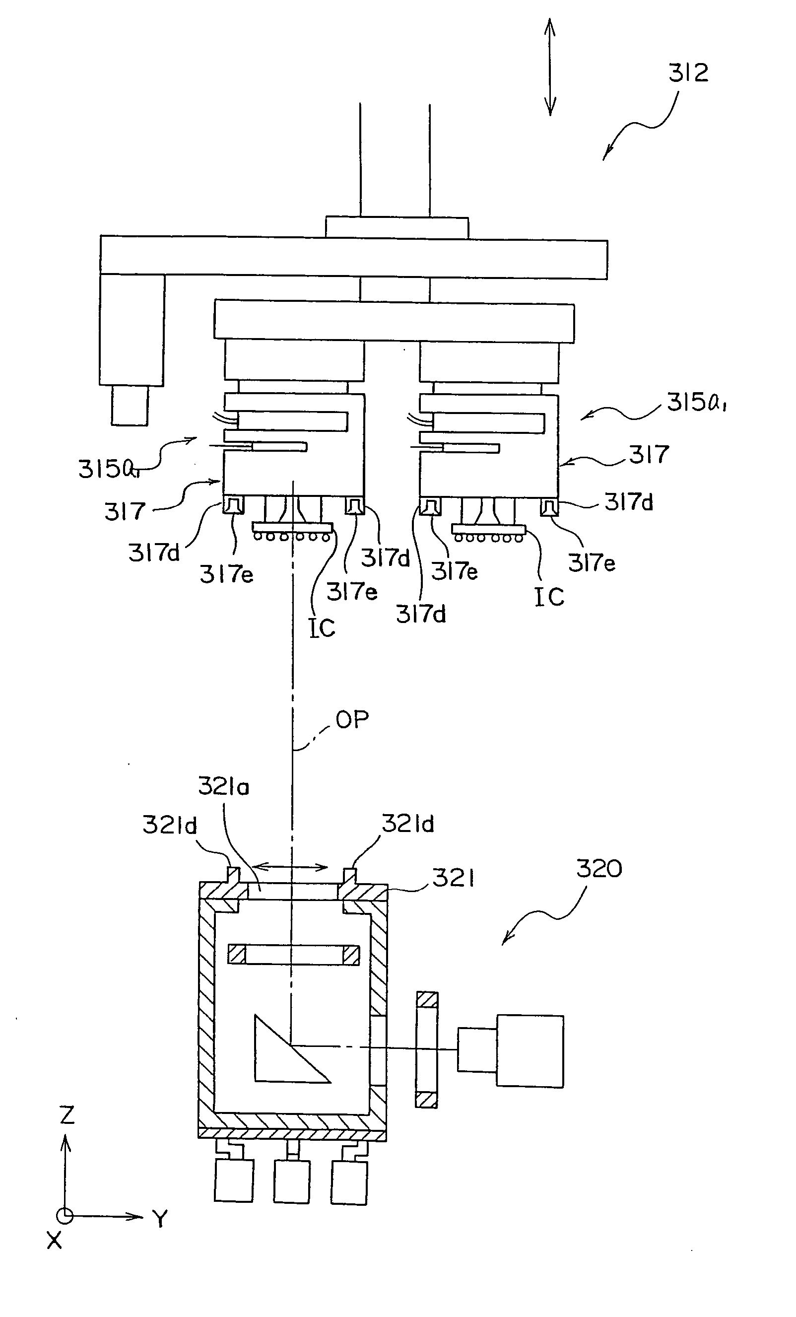
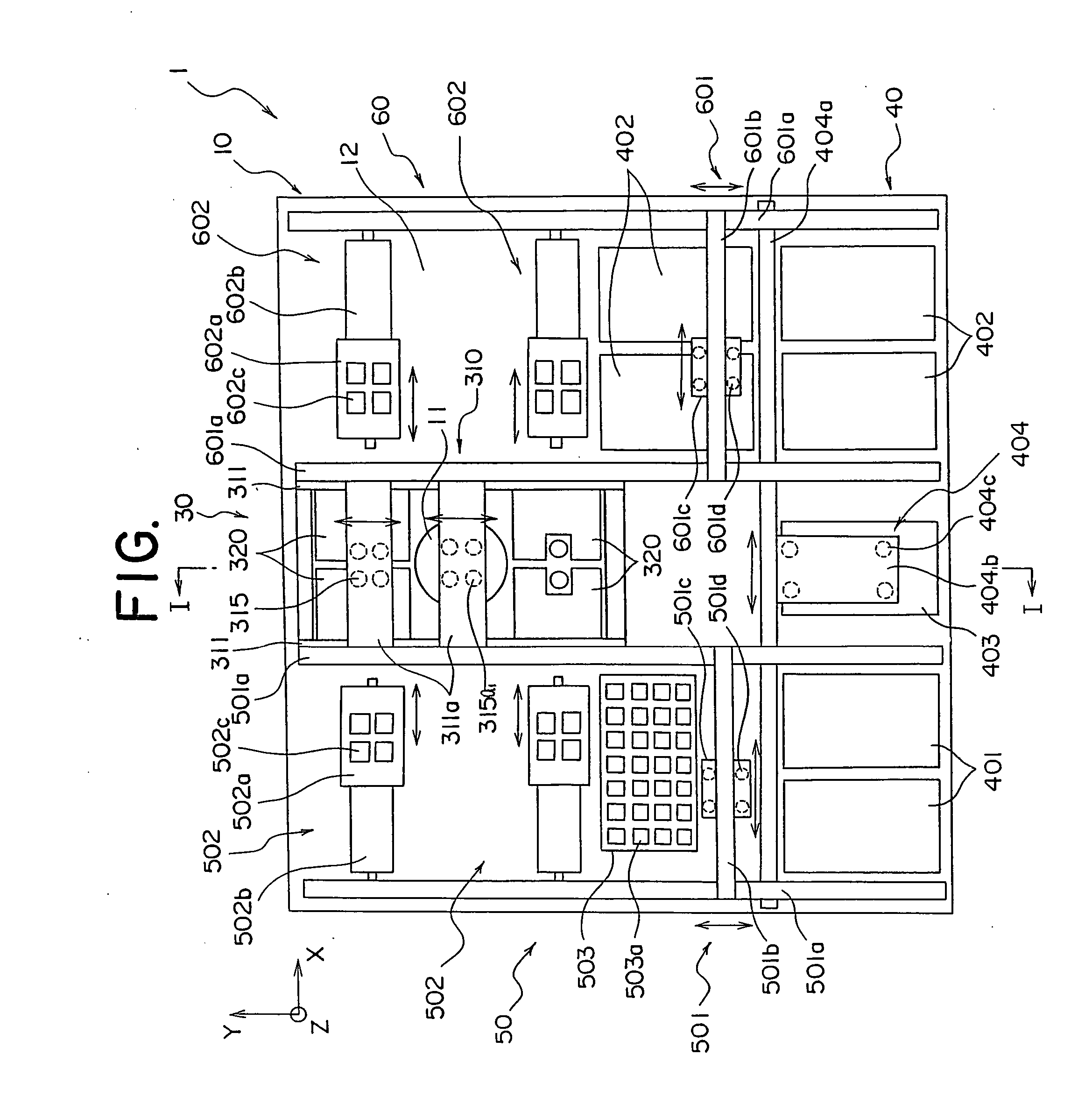
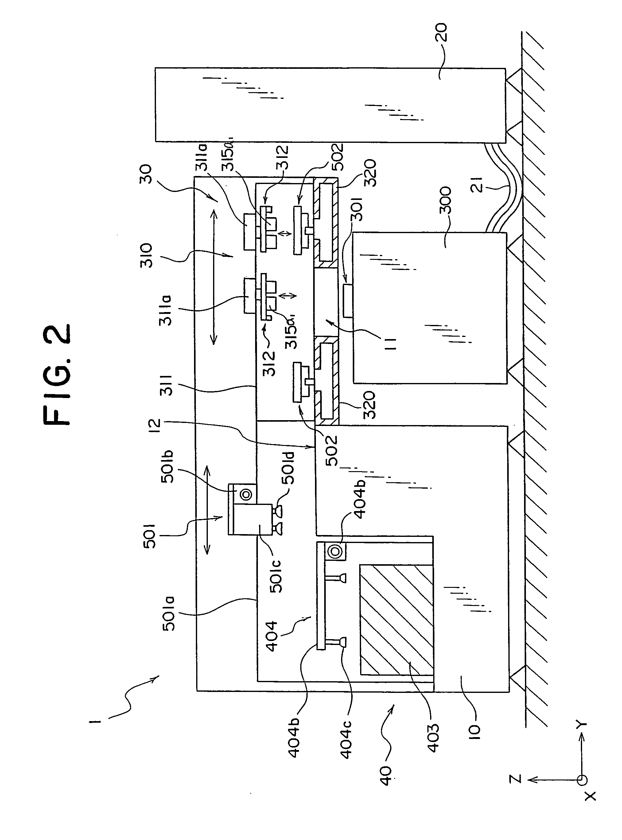
[0047] As shown in FIG. 1 and FIG. 2, an electronic device testing apparatus 1 in the first embodiment of the present invention comprises a handler 10, a test head 300 and a tester 20, wherein the test head 300 and the tester 20 are connected by a cable 21. Pre-test ICs on a supply tray held in a supply tray stocker 401 of the handler 10 are pressed against the contact portion 301 of the test head 300 by a YZ-transfer device 310 (moving means), and after being subjected to a test via the test head 300 and the cable 21, the post-test ICs are loaded on a classification trays held in a classification tray stocker 402 in accordance with the test result.

[0048] The handler 10 mainly comprises a test section 30, an IC magazine 40, a loader section 50 and an unloader section 60.

[0049] IC Magazine 40

[0050] The IC magazine 40 is a means for accommodating pre-test and post-test ICs and mainly comprises a supply tray stocker 401, a classification tray stocker 402, an empty tray stocker 403 an...

second embodiment

[0188] Below, as a second embodiment of the present invention, an embodiment wherein a plane following mechanism for naturally bringing ICs to be tested to contact the contact portion by making the contact arm follow a plane in parallel with the contact portion when the contact portion is inclined a little will be explained.

[0189] Note that the configuration of an electronic device testing apparatus except for the contact arm is the same as that in the above first embodiment, so that explanations on the configuration of the electronic device testing apparatus other than the contact arm will be omitted and the same reference numbers will be used for the same components as those in the first embodiment.

[0190] In the electronic device testing apparatus 1 in the present embodiment, as shown in FIG. 25, the movable head portion 312 of the YZ transfer device 310 of the test section 30 is provided with a base member 340 for supporting four first contact arms 315a2 arranged in two rows by...

third embodiment

[0226] In the above second embodiment, a case of providing two YZ transfer devices having four first contact arms in the test section was explained, but below, as a third embodiment, an electronic device testing apparatus wherein any number of first contact arms can be provided to the two YZ transfer devices will be explained.

[0227] Note that except that the number of the first contact arms is different, the configuration is the same as that of the electronic device testing apparatus in the above second embodiment, so that explanations on the configuration thereof other than the number of the first contact arm will be omitted and the same reference numbers will be used for the same components as those in the second embodiment.

[0228] In the electronic device testing apparatus 1 in the present embodiment, in the same way as in the second embodiment, the movable head portion 312 of the YZ transfer device 310 of the test section 30 is detachably attached with a unit composed of a base...


PUM


Abstract

A holding side contact arm (317) for holding an IC to be tested is positioned on the optical axis (OP) of an alignment CCD camera (326) of an alignment device (320), the IC to be tested is inserted to a first opening (321a) formed on an alignment movable portion (321), and a contact member (317d) of the holding side contact arm (317) is brought to contact the alignment movable portion (321). Then, an alignment amount for correcting a position of the IC to be tested is calculated by taking an image by the camera (326) and performing image processing. A lock-and-free means (318) provided to a first contact arm (315a1) is made to be in a non-restricted state, a movable portion driving device (322) is driven based on the alignment amount, and the holding side contact arm (317) contacting the alignment movable portion (321) is moved with respect to a root side contact arm (316), so that alignment of a position of the IC to be tested is performed.

Description

TECHNICAL FIELD [0001] The present invention relates to an electronic device testing apparatus for testing a semiconductor integrated circuit element and other various electronic devices (hereinafter, also representatively referred to as ICs), and particularly relates to an electronic device testing apparatus wherein erroneous contact is reduced. FIELD OF THE INVENTION [0002] In an electronic device testing apparatus called a handler, a large number of ICs to be tested held on a tray are conveyed into the handler, and the respective ICs to be tested are brought to electrically contact a test head for conducting a test by an electronic device testing apparatus body (hereinafter, also referred to as a tester). When the test is finished, the ICs are taken out from the test head and reloaded to trays in accordance with the test results so as to be classified to categories of good ones and defective ones, etc. [0003] In a conventional handler, a contact arm for bringing an electronic dev...

Claims


Application Information

Patent Timeline
IPC IPC(8): G01R31/26G01R31/01H01L21/66
CPCG01R31/01G01R31/2851G01R31/2893G01R31/2887G01R31/2886G01R31/26H01L22/00
Inventor OKUDA, HIROSHIKIYOKAWA, TOSHIYUKINAKAJIMA, HARUKI
Owner ADVANTEST CORP
Why Eureka
Try Eureka