Method of independent P and N gate length control of FET device made by sidewall image transfer technique

Inactive Publication Date: 2005-07-14
IBM CORP
View PDF9 Cites 166 Cited by
  • Summary
  • Abstract
  • Description
  • Claims
  • Application Information

AI Technical Summary

Benefits of technology

[0006] The invention provides a method of simultaneously forming different types of field effect transistors (e.g., N-type and P-type) on the same substrate. This method forms a conductive layer on a substrate and patterns sacrificial structures above the conductive layer. Next, the invention forms sidewall spacers adjacent the sacrificial structures using a spacer material capable of undergoing dimensional change, after which the invention removes the sacrificial structures in processing that leaves the sidewall spacers in place. The invention then protects selected ones of the sidewall spacers using a sacrificial mask and leaves th

Problems solved by technology

This processing dramatically simplifies and reduces the number of manufacturing steps required, and thereby incr

Method used


Image

  • Method of independent P and N gate length control of FET device made by sidewall image transfer technique
  • Method of independent P and N gate length control of FET device made by sidewall image transfer technique
  • Method of independent P and N gate length control of FET device made by sidewall image transfer technique

Examples


Example

[0017] The present invention and the various features and advantageous details thereof are explained more fully with reference to the nonlimiting embodiments that are illustrated in the accompanying drawings and detailed in the following description. It should be noted that the features illustrated in the drawings are not necessarily drawn to scale. Descriptions of well-known components and processing techniques are omitted so as to not unnecessarily obscure the present invention. The examples used herein are intended merely to facilitate an understanding of ways in which the invention may be practiced and to further enable those of skill in the art to practice the invention. Accordingly, the examples should not be construed as limiting the scope of the invention.

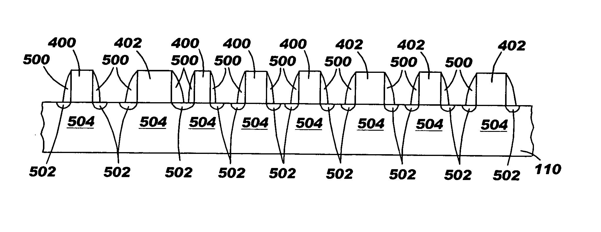
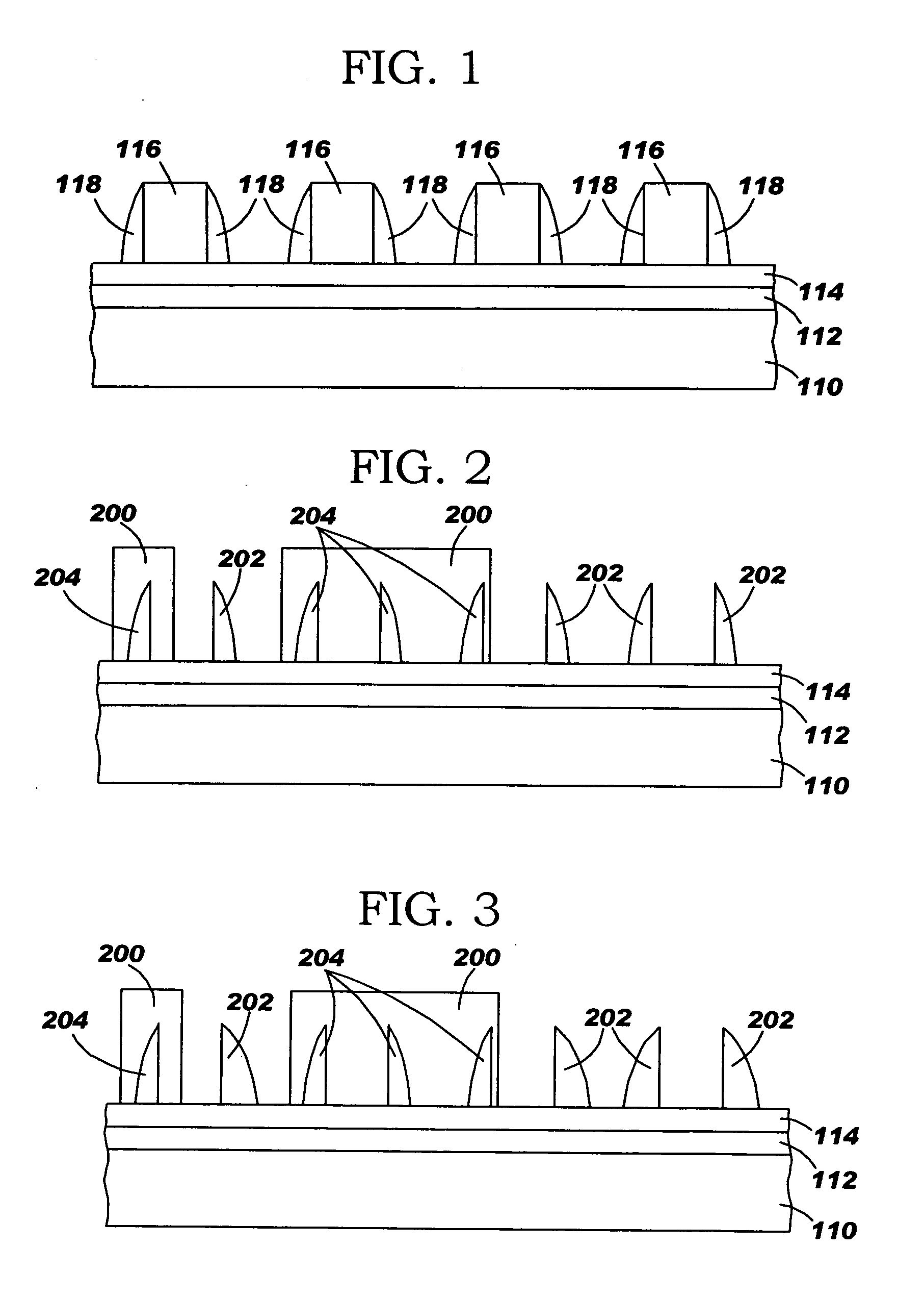
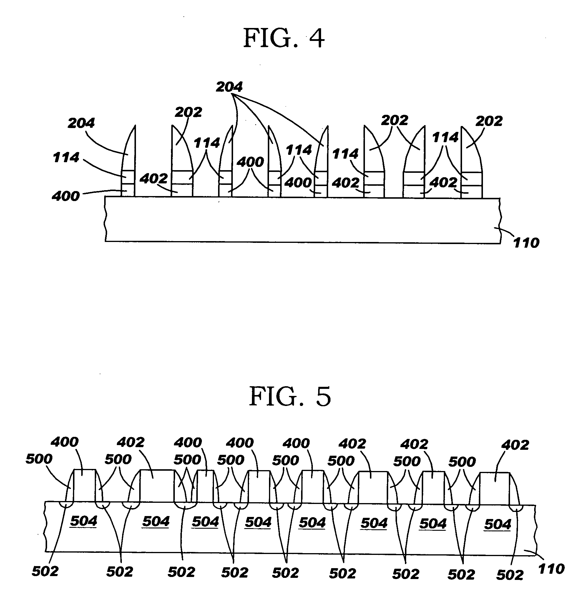
[0018] As shown in FIGS. 1-5, the invention provides a method of simultaneously forming different types of field effect transistors (e.g., N-type and P-type) on the same substrate. More specifically, as shown in FIG. 1, a ...


PUM


Abstract

Disclosed is a method that forms a conductive layer on a substrate and patterns sacrificial structures above the conductive layer. Next, the invention forms sidewall spacers adjacent the sacrificial structures using a spacer material capable of undergoing dimensional change, after which the invention removes the sacrificial structures in processing that leaves the sidewall spacers in place. The invention then protects selected ones of the sidewall spacers using a sacrificial mask and leaves the other ones of the sidewall spacers unprotected. This allows the invention to selectively expose the unprotected sidewall spacers to processing that changes the size of the unprotected sidewall spacers. This causes the unprotected sidewall spacers have a different size than protected sidewall spacers. Then, the invention removes the sacrificial mask and patterns the conductive layer using the sidewall spacers as a gate conductor mask to create differently sized gate conductors on the substrate. Following this, the invention removes the sidewall spacers and forms the source, drain, and channel regions adjacent the gate conductors.

Description

BACKGROUND OF THE INVENTION [0001] 1. Field of the Invention [0002] The present invention generally relates to a method of making independently optimized P and NFET devices with different gate lengths by SIT technique. The invention directly modifies the spacer width without the need for added resist etch processes. [0003] 2. Description of the Related Art [0004] As the industry pushes integrated circuit chip performance, the device gate length is being reduced to about half of the minimum lithographic dimension, and is still shrinking. Such sublithographic gate dimensions are achieved by trimming the etching mask (either hard mask or photoresist) of the gate material before the gate material etch. However, the tolerance of this method is inherently unstable because of the difficulty in controlling the photolithography and etch dimensions, as well as the trim dimension. [0005] Sidewall image transfer (SIT) has been known to produce FET devices of sublithographic dimensions with supe...

Claims


Application Information

Patent Timeline
IPC IPC(8): H01L21/033H01L21/28H01L21/3213
CPCH01L21/0337H01L21/32139H01L21/2815
Inventor FURUKAWA, TOSHIHARUHOLMES, STEVEN J.MA, WILLIAM H-L
Owner IBM CORP
Why Eureka
Try Eureka