Method of fabricating microelectronic device using super critical fluid

a microelectronic device and super critical fluid technology, applied in the direction of electrical cables, cable fittings, electrical cables, etc., can solve the problems of parasitic capacitance, poor transmission of electric signals through metal interconnections, and discontinuity of layers

Active Publication Date: 2005-07-14
SAMSUNG ELECTRONICS CO LTD
View PDF12 Cites 40 Cited by
  • Summary
  • Abstract
  • Description
  • Claims
  • Application Information

AI Technical Summary

Benefits of technology

[0021] In accordance with still another exemplary embodiment, the present invention provides a method of fabricating a microelectronic device which includes a step of preparing a substrate having a lower interconnection. An etch stop layer is formed for covering the lower interconnection. An interlayer insulating layer, which is composed of a low-k dielectric material, is formed on the etch stop layer. The interlayer insulating layer is etched until the etch stop layer is exposed, thereby forming an opening inside the interlayer insulating layer. The opening includes a via exposing the etch stop layer at a bottom thereof, and a preliminary trench extending from the via. A sacrificial layer, which is composed of a HSQ based material, is formed for filling at least a portion of the opening. A photoresist pattern is formed for exposing the sacrificial layer and the interlayer insulating layer around the opening. The interlayer insulating layer and the sacrificial layer, which are exposed after the photoresist pattern is formed, are etched, thereby forming a trench extending from the preliminary trench. The sacrificial layer and the photoresist pattern are then concurrently removed using super critical CO2. The etch stop layer is thereafter removed, thereby exposing the lower interconnection. The via and the trench are next filled with a conductive layer, thereby forming an upper interconnection, which is connected to the lower interconnection through the via.
[0022] These and other useful embodiments of this invention will be described below in reference to the several drawings.

Problems solved by technology

The conventional formation method of a dual damascene interconnection described as above has a number of problems and limitations, including the facts that a leakage current is normally increased, and the seed layer and the diffusion barrier layer are usually poorly deposited, thereby causing discontinuity of layers, due to the effects of the wet etching process for removing the sacrificial layers 16a, 16b, during which the capping layer 15a may be reduced in width and / or lifted.
However, if the distance between metal interconnections becomes too narrow, a cross talk may occur between the metal interconnections, and a parasitic capacitance between the metal interconnections having the insulating layer formed therebetween is thereby increased.
As a result, electric signals through the metal interconnections are poorly transmitted, or a transmission speed of such signals is reduced.
Such formation method has a problem, however, in that silanol groups are formed inside the low-k dielectric interlayer insulating layer 14a of porous property during the wet etching process of removing the sacrificial layers 16a, 16b, thereby increasing a dielectric constant.

Method used


Image

  • Method of fabricating microelectronic device using super critical fluid
  • Method of fabricating microelectronic device using super critical fluid
  • Method of fabricating microelectronic device using super critical fluid

Examples


Embodiment Construction

[0029] The present invention will now be described more fully hereinafter with reference to the accompanying drawings, in which preferred embodiments of the invention are shown. It will be understood, however, that this invention may be embodied in many different forms and should not be construed as being limited to the embodiments set forth herein. Rather, these embodiments are provided so that this disclosure will be thorough and complete, and will fully convey the scope of the invention to those skilled in the art. In the drawings, the thicknesses of layers and regions are exaggerated for clarity. Like numbers refer to like elements throughout the specification.

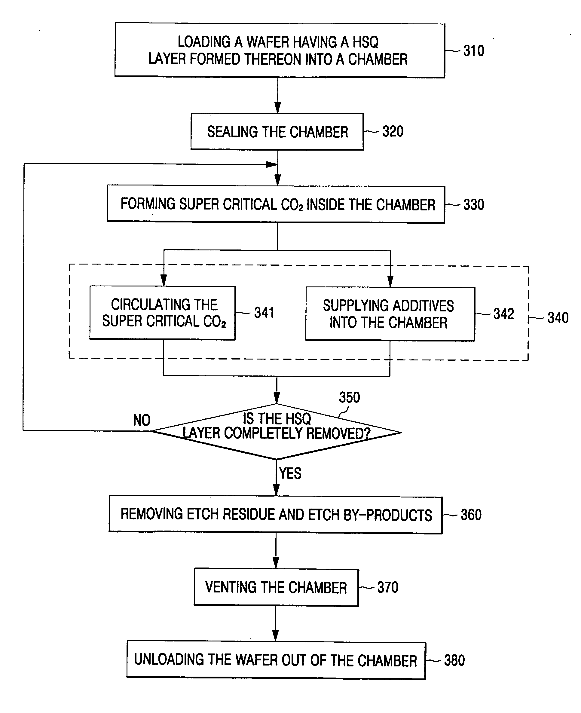
[0030] Embodiments of the present invention provide a method of removing a material layer using super critical fluid as part of a novel fabrication technique for preparing microelectronic devices. As shown in FIG. 2, there exists a fourth phase state besides the familiar solid, liquid, and gas phase states of a material; ...


PUM


Abstract

Methods of fabricating a microelectronic device having improved performance characteristics are disclosed which are characterized by using super critical fluid to perform a material removal step. In one illustrative embodiment, the method includes preparing a substrate, forming an HSQ layer covering at least a portion of the substrate, and thereafter removing at least portions of the HSQ layer using super critical fluid CO2.

Description

CROSS-REFERENCE TO RELATED APPLICATION [0001] This application claims the benefit of Korean Patent Application No. 2004-2754, filed on Jan. 14, 2004, the disclosure of which is hereby incorporated herein by reference in its entirety. BACKGROUND OF THE INVENTION [0002] 1. Field of the Invention [0003] The present invention relates to a method of fabricating a microelectronic device, and more particularly, to a method of fabricating a microelectronic device using super critical fluid. [0004] 2. Discussion of the Related Art [0005] A microelectronic device such as a highly-integrated semiconductor device is structured such that elements in its upper and lower portions are connected to each other via a multilayer structure of metal interconnections. Since a metal layer is relatively difficult to etch in comparison with an insulating layer, a dual damascene process is used to pattern the metal layer. U.S. Pat. No. 6,057,239, by Fei Wang, et. al. which is incorporated herein by reference,...

Claims


Application Information

Patent Timeline
Patent Type & Authority Applications(United States)
IPC IPC(8): H01L21/3205H01L21/00H01L21/302H01L21/461H01L21/768H01L21/8242
CPCH01L21/76802H01L21/76835H01L21/76829H01L21/76808H01B13/22H02G15/064
Inventor HAN, SANG-CHEOLOH, JUN-HWAN
Owner SAMSUNG ELECTRONICS CO LTD
Why Eureka
Try Eureka