

Filter assembly, method of manufacturing the same, and plasma display panel using the same
- Summary
- Abstract
- Description
- Claims
- Application Information
AI Technical Summary
Benefits of technology
Problems solved by technology
Method used
Image

Examples
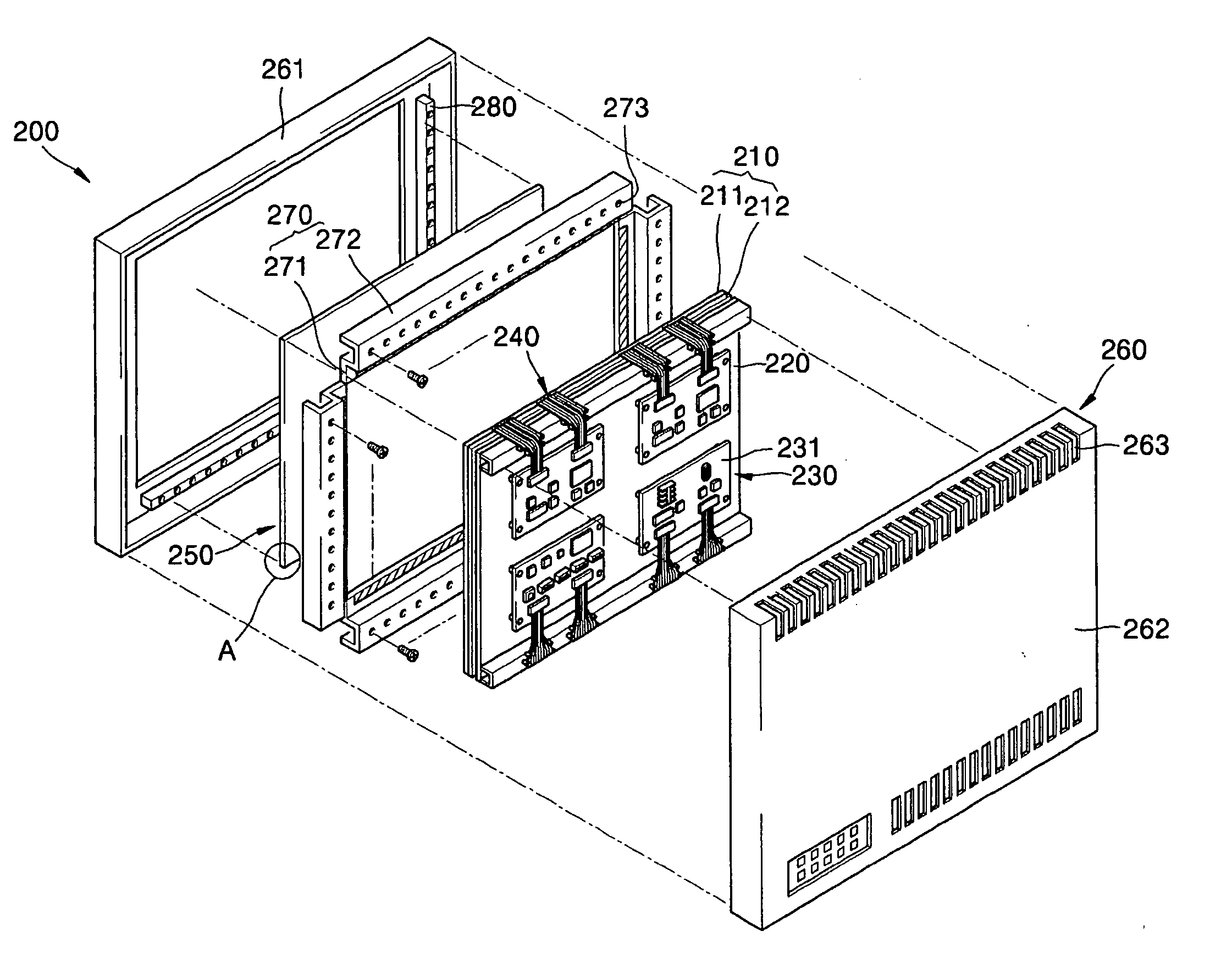
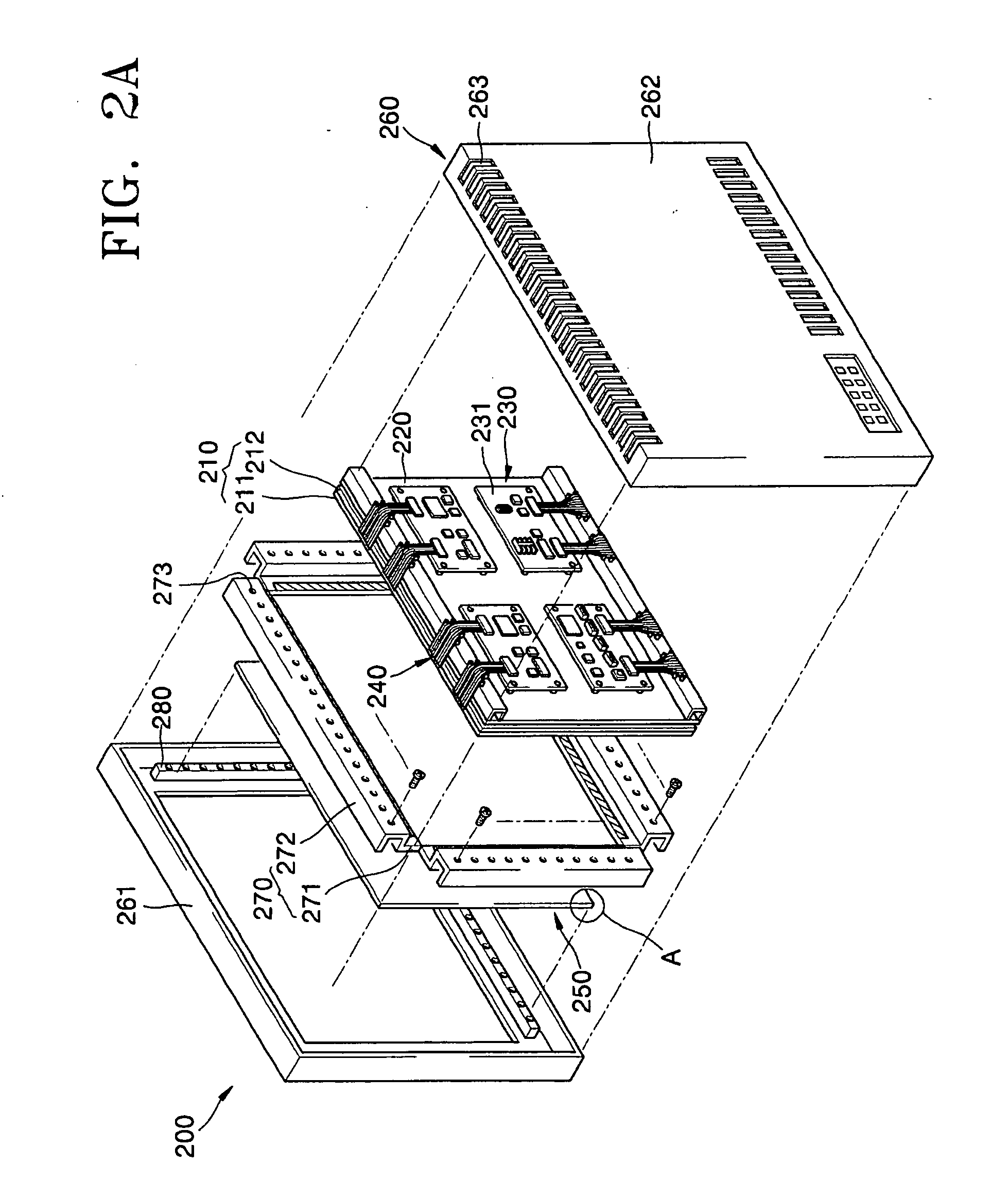
case 260
[0039] Case 260 includes a rear cabinet 262 that is perforated by ventilation holes and the front cabinet 261. Case 260 accommodates the panel assembly 210, the chassis base 220, and the filter assembly 250 between the front cabinet 261 and the rear cabinet 262.
[0040] A substrate 251 formed of transparent glass or plastic and included in the filter assembly 250. An anti-reflection film 252 for preventing the reduction of visibility due to the reflection of external light is attached on a front surface of the transparent substrate 251. The anti-reflection film 252 is treated with an anti-reflection (AR) processing. An electromagnetic wave shielding filter 253 is an electromagnetic interference (EMI) shielding filter for shielding electromagnetic waves generated from the plasma display panel 200 during driving thereof is located on a rear surface of the transparent substrate 251. A selected wave absorption film 254 is attached on a surface of the electromagnetic wave shielding filter....
PUM
| Property | Measurement | Unit |
|---|---|---|
| Thickness | aaaaa | aaaaa |
| Density | aaaaa | aaaaa |
| Dimensionless property | aaaaa | aaaaa |
Abstract
Description
Claims
Application Information