Method and apparatus for measuring optical overlay deviation

a technology of optical overlay and measurement method, applied in the direction of photomechanical apparatus, instruments, optics, etc., can solve the problem that the optical overlay can suffer from magnification wis, and achieve the effect of improving the overlay measurement accuracy

Active Publication Date: 2005-07-21
NIKON CORP
View PDF7 Cites 35 Cited by
  • Summary
  • Abstract
  • Description
  • Claims
  • Application Information

AI Technical Summary

Benefits of technology

[0013] Accordingly, one aspect of the present invention is to provide apparatus and methods that can characterize and monitor WIS in real time in order to improve the overlay measurement accuracy.
[0014] According to one aspect of the invention, an apparatus and method for measuring overlay deviation between two layers is capable of evaluating WIS in a simple manner without necessarily requiring AEI. A wafer having alignment marks provided in two layers is placed on a stage device that is movable in X, Y, Z and θ directions. The substrate is provided in the X-Y plane, and the Z-axis is perpendicular to the substrate surface (i.e., the X-Y plane). The apparatus can measure TIS at substrate orientations of 0° and 180°, and calculate TCV for each alignment mark. The apparatus also measures TIS-through-focus (i.e., TIS at different focus positions) by moving the wafer along the Z-axis and calculating TIS at a plurality of Z-axis positions. TCV-through-focus (i.e., TCV values at the different focus positions) can be calculated for each alignment mark using the values obtained for TIS-through-focus. If the layers formed on the substrate suffer from WIS, the TCV values will change at different Z-axis positions (i.e., at different focus positions) of the substrate. The present invention, thus, can display a vector map of the TCV-through-focus values so that an observer of the vector map can determine whether the wafer suffers from WIS.

Problems solved by technology

However, when the d / dz TIS vector-map shows a directional component and the d / dz TCV vector-map shows a magnification component, the wafer can be deemed to suffer from magnification WIS.

Method used


Image

  • Method and apparatus for measuring optical overlay deviation
  • Method and apparatus for measuring optical overlay deviation
  • Method and apparatus for measuring optical overlay deviation

Examples


Embodiment Construction

[0032] A preferred exemplary embodiment of the invention will be described with reference to the drawings.

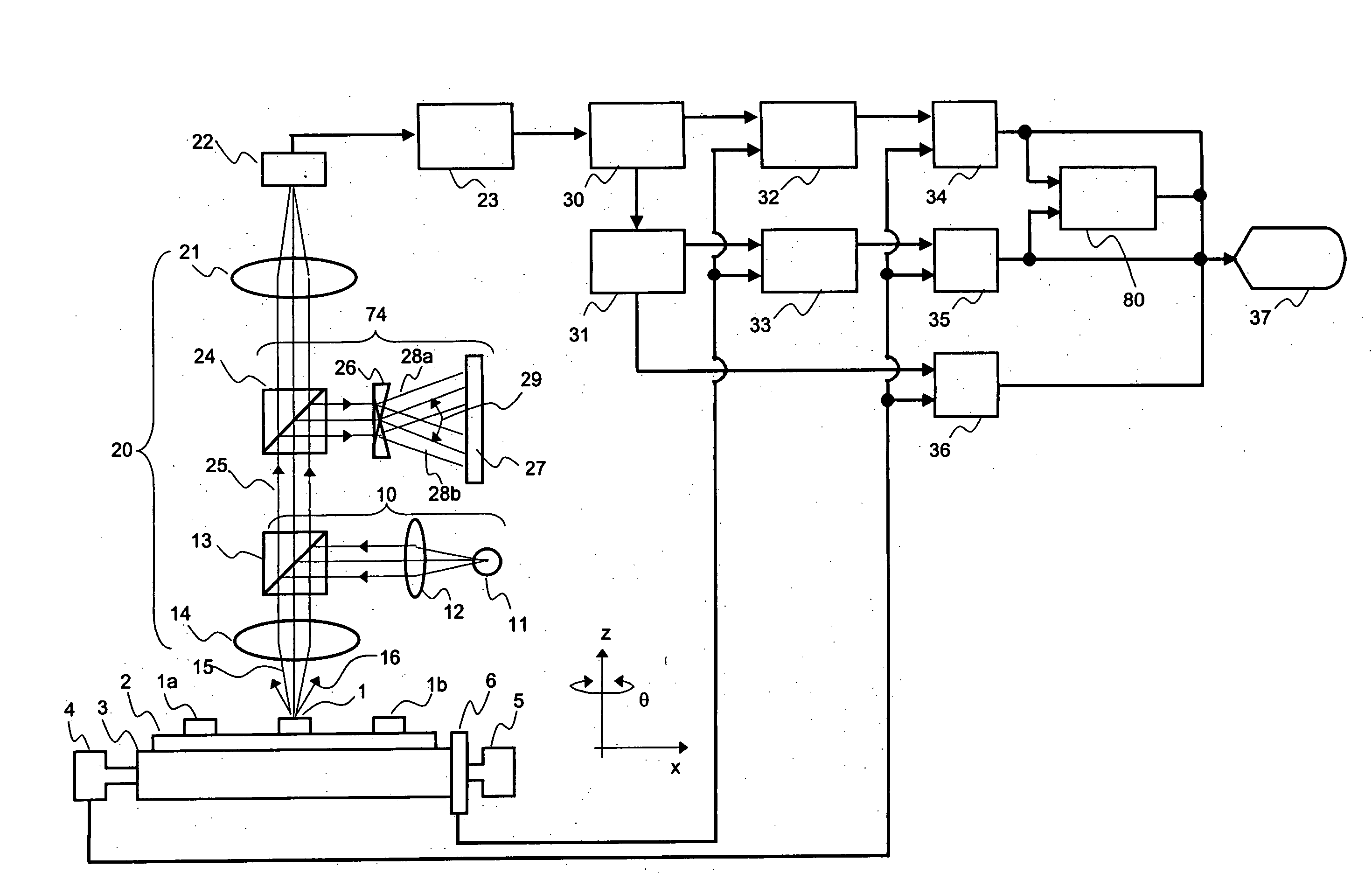
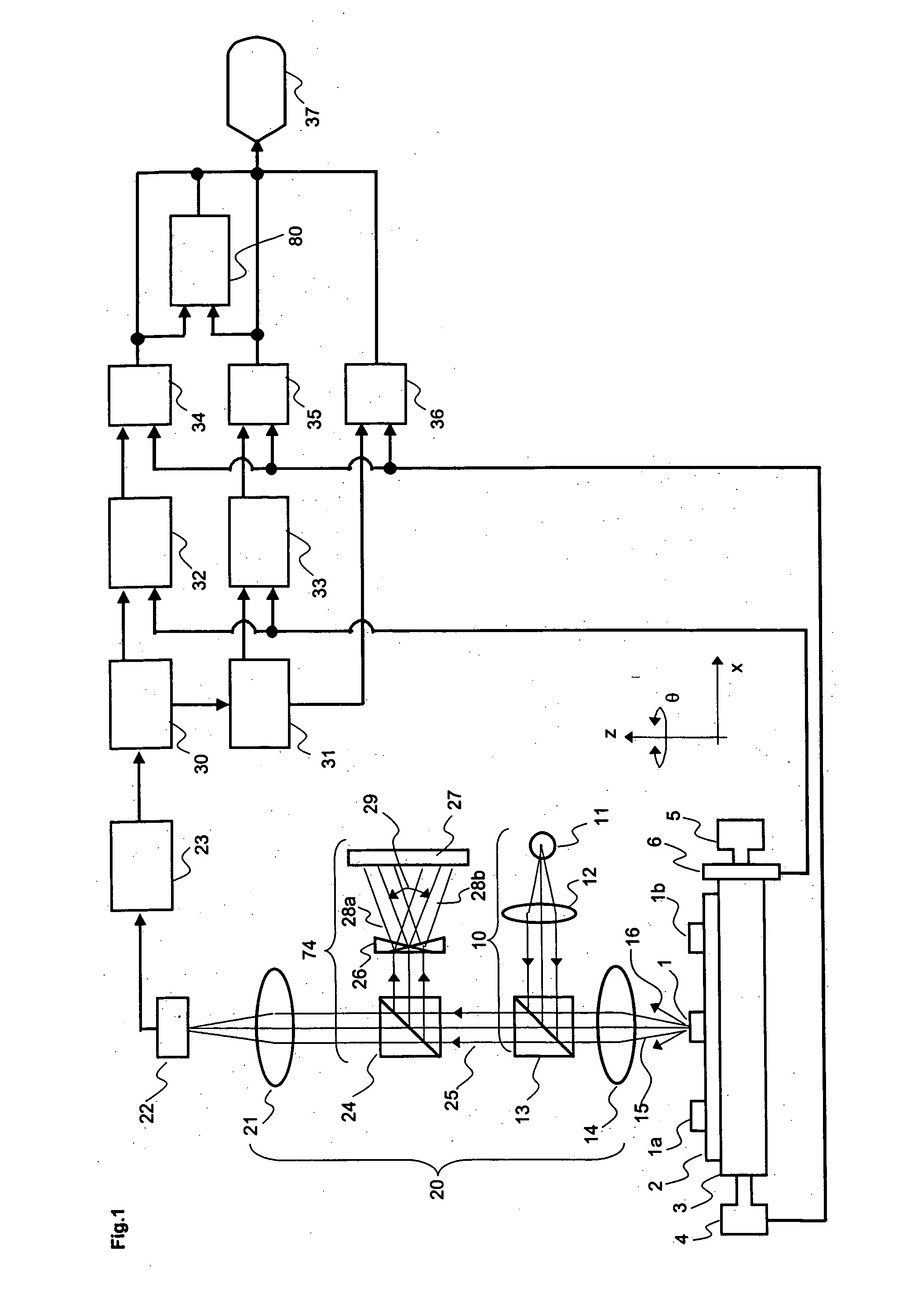
[0033]FIG. 1 shows one example of an apparatus for measuring an overlay-offset according to the present invention. A direction perpendicular to the sheet surface is set as the Y-axis direction, directions extending to the right and left are set as the X-axis direction, and directions extending up and down are set as the Z-axis directions. Rotation about the Z-axis is set as θ in FIG. 1.

[0034] The measuring apparatus measures overlay-offset, i.e., a positional deviation in alignment of an alignment mark 1 formed on a substrate such as wafer 2. As is known, there are many alignment marks 1a and 1b on the wafer 2. The wafer 2 is placed on a stage 3 during measurement of the overlay-offset. The stage 3 is movable in X and Y-directions, and is rotatable in the θ direction (i.e., about the Z-axis). Thus, overlay-offset can be measured for a wafer at a 0° orientation and at a 180° or...


PUM

PropertyMeasurementUnit
optical overlay deviation measurementaaaaaaaaaa
optical inspectionaaaaaaaaaa
dimensionsaaaaaaaaaa

Abstract

An apparatus and method analyze overlay deviation in alignment between a first mark and a second mark that are formed on a substrate. In particular, a relationship between changes in overlay deviation values and changes in focus position of the substrate for a plurality of sets of the first and second marks that are provided on the substrate is calculated, and then an output is provided from which a user can determine whether the substrate suffers from wafer-induced-shift. Preferably, the output is a vector-map showing the relationship between changes in overlay deviation values and changes in focus position of the substrate for the plurality of sets of marks.

Description

BACKGROUND OF THE INVENTION [0001] 1. Field of Invention [0002] The present invention relates generally to optical inspection of semiconductor substrates during the production of semiconductor devices. In particular, the present invention relates to methods and apparatus for detecting the overlay deviation between two patterned layers on a semiconductor substrate. [0003] 2. Description of Related Art [0004] One of the most critical process control techniques used in the manufacturing of integrated circuits is the measurement of overlay accuracy between patterned layers, i.e., the measurement of how accurately a patterned layer aligns with respect to another patterned layer located (directly or indirectly) above or below that layer. [0005] Overlay measurement typically is performed on a patterned resist layer prior to etching that layer. If a substrate contains layers that are out of alignment, then the substrate should be reworked (i.e., the photoresist layer(s) are stripped) and re...

Claims


Application Information

Patent Timeline
Patent Type & Authority Applications(United States)
IPC IPC(8): G01B11/00G03F7/20G03F9/00H01L21/027
CPCG03F7/70633
Inventor HAYANO, FUMINORI
Owner NIKON CORP
Why Eureka
Try Eureka