Semiconductor laser and manufacturing method therefor

Inactive Publication Date: 2005-07-21
SHARP KK
View PDF8 Cites 14 Cited by
  • Summary
  • Abstract
  • Description
  • Claims
  • Application Information

AI Technical Summary

Benefits of technology

[0009] An object of the present invention is to provide a semiconductor laser which is capable of emitting laser light with low aspect ratio without generating kink even during high-output operation, little power dependency of an horizontal beam divergence θh between a low-output operation and a high-output operation, low loss so as to allow the high-output operation, capable of offering a horizontal radiation light distribution close to Gaussian distribution, and excellent efficiency in use for optical disks, and a manufacturing method therefor.

Problems solved by technology

It is difficult in manufacturing process to gradually change the thickness of a section from the upper cladding layer to the lower surface of the buried layer on both sides of the ridge stripe region.

Method used


Image

  • Semiconductor laser and manufacturing method therefor
  • Semiconductor laser and manufacturing method therefor
  • Semiconductor laser and manufacturing method therefor

Examples


first embodiment

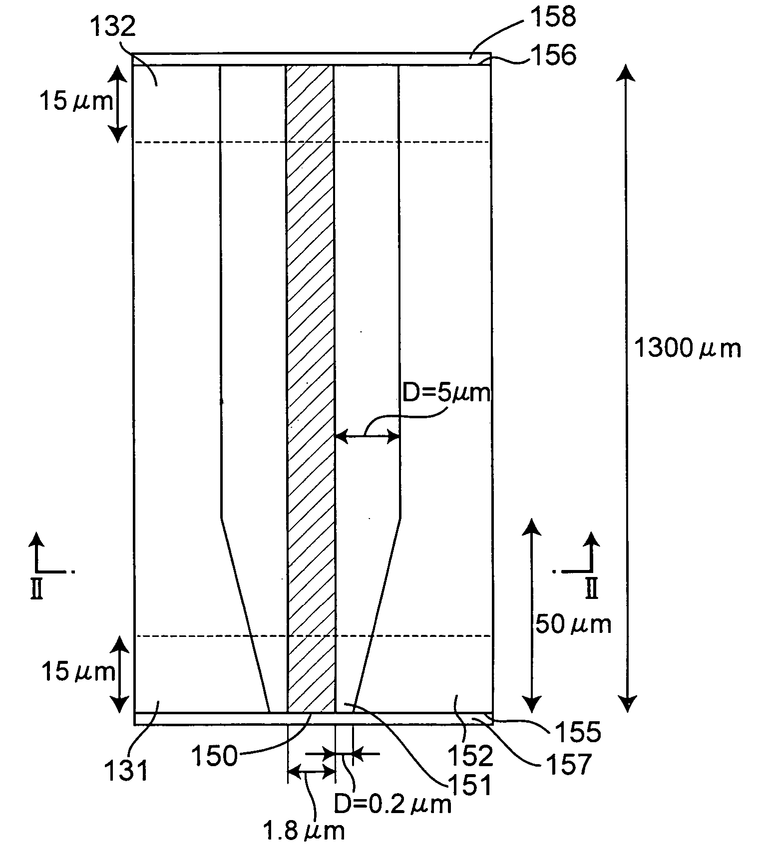
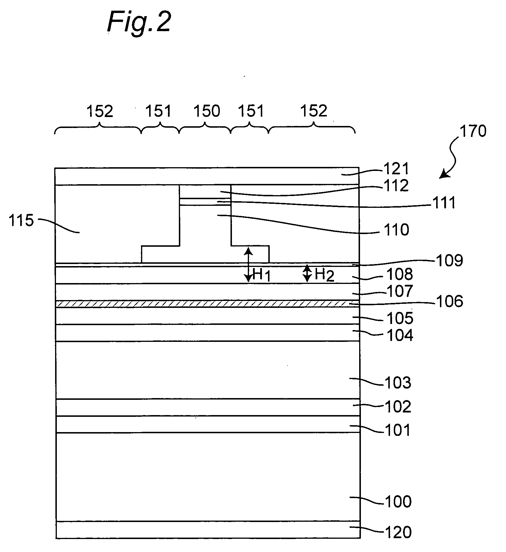
[0045]FIG. 1 is a schematic top view showing a preferred example of the present invention. As shown in FIGS. 1 and 2, a semiconductor laser of the present invention is provided with a laminated structure 170, a ridge stripe region 150, a first stripe-side region 151 and a second stripe-side region 152. The first stripe-side regions 151 are provided on both outer sides of the ridge stripe region 150, and the second stripe-side regions 152 are provided on both outer sides of the first stripe-side regions 151. The second stripe-side region 152 is extremely adjacent to the ridge stripe region 150 in the vicinity of a light emitting edge 155. Although a width D of the first stripe-side region is set at 0.2 μm in this example, it may be about 0.1 to 0.5 μm for example. The width D of the first stripe-side region 151 is gradually increased from the light emitting edge 155 to form a taper-shape, and becomes constant in the inside portion of an oscillator. The width D of the first stripe-sid...

second embodiment

[0062]FIG. 4 is a schematic top view showing a second embodiment of the present invention. As shown in FIGS. 4 and 5, a second semiconductor laser is provided with a laminated structure 270, a ridge stripe region 250, a first stripe-side region 251, and a second stripe-side region 252. Further, in the range of 15 μm from a light emitting front edge 255 and a light emitting rear edge 256, window regions 231, 232 are formed respectively. The second stripe-side region 252 is extremely adjacent to the ridge stripe region 250 in the vicinity of the light emitting front edge 255, and a width D of the first strip-side region is about 0.3 μm herein. The width D of the first stripe-side region 251 is rapidly increased in the vicinity of the boundary of the window regions, and the second stripe-side region 252 is not present in the inner side of an oscillator from the window regions 231, 232.

[0063]FIG. 5 is a cross sectional view taken along the line V-V of the semiconductor laser shown in F...

third embodiment

[0076]FIG. 6 is a schematic top view showing a third embodiment of the present invention. As shown in FIGS. 6 and 7, a semiconductor laser of the present embodiment is provided with a laminated structure 370, ridge stripe region 350, first stripe-side region 351, and a second stripe-side region 352. The second stripe-side region 352 is extremely adjacent to the ridge stripe region 350 in the vicinity of a light emitting edge 355, and the width D of the first strip-side region is herein set at about 0 to 0.5 μm, preferably about 0.05 to 0.2 μm. The width D of the first stripe-side region is gradually increased preferably from the light emitting edge 355, and becomes 5 μm in a position 100 μm away from oscillator edges. If the width is 5 μm or more, then the second stripe-side region 352 has substantially no influence on a guided wave. In the range of 15 μm from the light emitting front edge 355 and light emitting rear edge 356, window regions 331, 332 are respectively formed.

[0077]F...


PUM


Abstract

A semiconductor laser has a ridge stripe region 150 with laminated structure 170 and first and second stripe-side regions 151, 152. The ridge stripe region 150 on a semiconductor substrate has a lower cladding layer, active layer, and upper cladding area. The first stripe side regions 151 are disposed on both outer sides of a ridge stripe region 150. The second stripe-side regions are disposed on both outer sides of the first stripe-side regions 151. A thickness from a lower surface of the upper cladding region to a lower surface of a buried layer 115 in the second stripe-side region is smaller than that in the first stripe-side region. A width of the first stripe side region 151 is larger in a middle portion of an oscillator than in a light emitting edge.

Description

RELATED APPLICATION [0001] This application is based on Japanese Patent Application No. 2004-8875, the contents in which are incorporated herein by reference. BACKGROUND OF THE INVENTION [0002] The present invention relates to a semiconductor laser and a manufacturing method therefor, and more particularly relates to a semiconductor laser and a manufacturing method therefor suitable for data write onto optical disks and data read from optical disks (hereinbelow referred to as “for optical disks”). [0003] Conventionally, as semiconductor lasers in use for optical disks, the semiconductor lasers which emit laser light from their edges have been used. The semiconductor lasers for optical disks require laser light capable of offering a spot shape which is as close to a perfect circle as possible on an optical disk. Typically, the laser light has an elliptic cross section, and its aspect ratio of beam divergence is defined as θv / θh wherein θh represents a full-width at half maximum of ho...

Claims


Application Information

Patent Timeline
IPC IPC(8): H01S5/22H01S5/00H01S5/10H01S5/16H01S5/223H01S5/30H01S5/34H01S5/343
CPCB82Y20/00H01S5/1014H01S5/1039H01S2301/18H01S5/2231H01S5/3436H01S5/16
Inventor WATANABE, MASANORI
Owner SHARP KK
Why Eureka
Try Eureka