Semiconductor device and method of fabricating the same

a semiconductor and insulating layer technology, applied in the direction of chemistry apparatus and processes, water/sewage treatment by ion exchange, specific water treatment objectives, etc., can solve the problems of deteriorating the reliability of adhesion of silicon substrates to base plates, adversely affecting adhesive force, etc., to improve the reliability of adhesion of semiconductor constructing bodies

Inactive Publication Date: 2005-07-28
AOI ELECTRONICS CO LTD
View PDF20 Cites 43 Cited by
  • Summary
  • Abstract
  • Description
  • Claims
  • Application Information

AI Technical Summary

Benefits of technology

[0007] It is, therefore, an object of the present invention to provide a semiconductor device and a method of fabricating the same which can improve the reliability of adhesion of a semiconductor constructing body to a base member.
[0019] In these aspects, the semiconductor constructing body is directly fixed to the base member made of the material containing at least a thermosetting resin. Since no such adhesive layer as used in the conventional device is used, the semiconductor device can be made thin accordingly. In addition, the reliability of adhesion of the semiconductor constructing body to the base member can be improved.

Problems solved by technology

This adversely affects the adhesive force, and deteriorates the reliability of adhesion of the silicon substrate to the base plate.

Method used


Image

  • Semiconductor device and method of fabricating the same
  • Semiconductor device and method of fabricating the same
  • Semiconductor device and method of fabricating the same

Examples


first embodiment

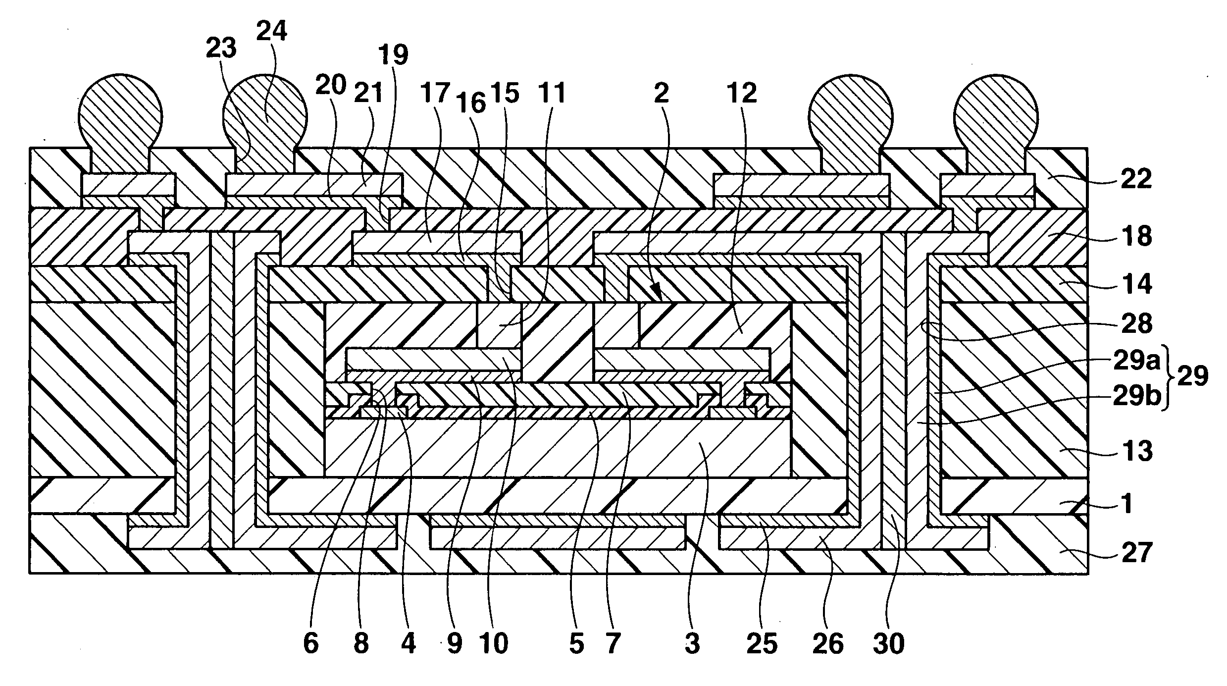
[0043]FIG. 1 is a sectional view of a semiconductor device according to the first embodiment of the present invention. This semiconductor device includes a base plate (base member) 1 having a square or rectangular planar shape. The base plate 1 is obtained by hardening a thermosetting resin containing reinforcing materials into the form of a sheet. Although the material of the base plate 1 is not limited, a preferred example is a material called a prepreg material obtained by impregnating a substrate formed by a fiber-like reinforcing material, e.g., fibers made of an inorganic material such as glass or aramid fibers, with a thermosetting resin such as an epoxy-based resin, and semi-hardening the resultant substrate (by B-stage hardening).

[0044] The lower surface of a semiconductor constructing body 2 having a square or rectangular planar shape and a size smaller to a certain degree than the size of the base plate 1 is directly fixed to the upper surface of the base plate 1. The se...

second embodiment

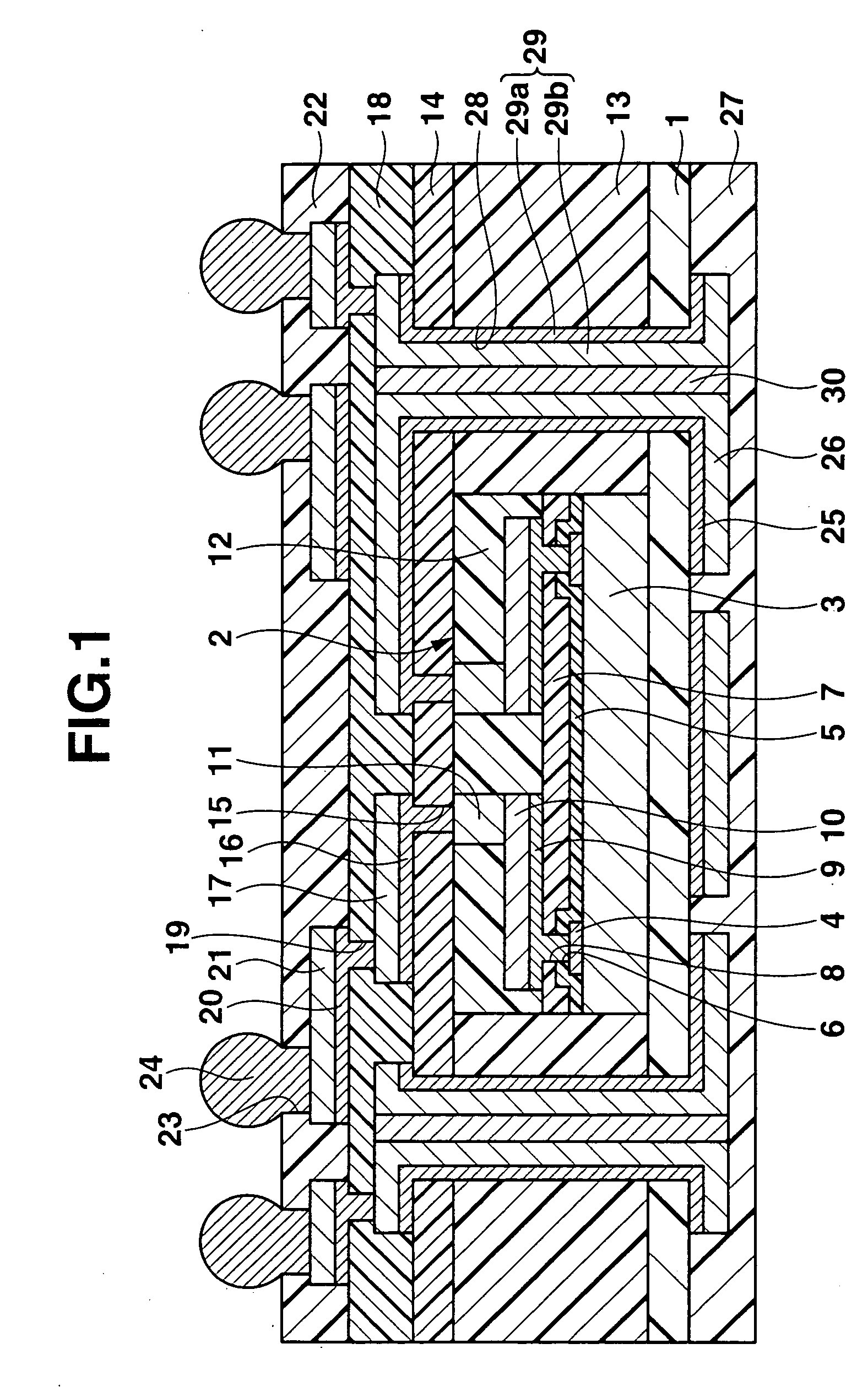
[0081]FIG. 17 is a sectional view of a semiconductor device according to the second embodiment of the present invention. This semiconductor device differs from that of the first embodiment in that lower interconnections 26 including a lower metal undercoating 25 are formed on the entire lower surface of a metal layer 31 formed by copper or the like on the lower surface of a base plate 1, and the thickness of the base plate 1 made of a prepreg material is made smaller to some extent than that in the first embodiment.

[0082] When the semiconductor device of the second embodiment is to be fabricated, in the step shown in FIG. 10, as shown in FIG. 18, a metal layer 31 made of a copper foil or copper plate is placed on the lower surface of a base plate formation sheet 1a, and fixed to the lower surface of a base plate 1 by heating and pressing from above and below by a pair of heating / pressing plates 45 and 46. In this case, the metal layer 31 also has the function of a support plate whi...


PUM


Abstract

A semiconductor device includes a base member made of a material containing at least a thermosetting resin, and at least one semiconductor constructing body mounted on the base member, and having a semiconductor substrate and a plurality of external connecting electrodes formed on the semiconductor substrate. An insulating layer is formed on the base member around the semiconductor constructing body. An interconnection of at least one layer is formed on one sides of the semiconductor constructing body and insulating layer, electrically connected to the external connecting electrode of the semiconductor constructing body, and having a connecting pad portion, the semiconductor substrate is fixed to the base member by fixing force of the base member.

Description

CROSS-REFERENCE TO RELATED APPLICATIONS [0001] This application is based upon and claims the benefit of priority from prior Japanese Patent Application No. 2004-018536, filed Jan. 27, 2004, the entire contents of which are incorporated herein by reference. BACKGROUND OF THE INVENTION [0002] 1. Field of the Invention [0003] The present invention relates to a semiconductor device and a method of fabricating the same. [0004] 2. Description of the Related Art [0005] The conventional semiconductor device disclosed in Jpn. Pat. Appln. KOKAI Publication No. 2003-298005 (P2003-298005A) includes solder balls as connecting terminals for external connection outside the size of a silicon substrate. Therefore, this semiconductor device has a structure in which a silicon substrate having a plurality of connecting pads on its upper surface is adhered to the upper surface of a base plate via an adhesive layer, an insulating layer is formed on the upper surface of the base plate around the silicon s...

Claims


Application Information

Patent Timeline
Patent Type & Authority Applications(United States)
IPC IPC(8): H01L21/3205H01L21/44H01L23/52H01L21/60H01L23/053H01L23/12H01L23/31H01L23/485H01L23/538H01L25/04H01L25/18
CPCH01L23/3114H01L2224/0401H01L23/5389H01L24/24H01L24/82H01L2224/24226H01L2224/82039H01L2224/82047H01L2924/01013H01L2924/01029H01L2924/01057H01L2924/01074H01L2924/01078H01L2924/14H01L2924/15311H01L2924/01005H01L2924/01006H01L2924/01033H01L2924/01047H01L2924/014H01L23/3128H01L2224/97H01L2224/92244H01L2224/73267H01L2224/32225H01L2224/12105H01L2224/04105H01L24/97H01L2224/82H01L2224/83H01L2924/00H01L2924/12042C02F1/42C02F2303/22C02F2201/004
Inventor MIHARA, ICHIRO
Owner AOI ELECTRONICS CO LTD
Why Eureka
Try Eureka