Heat dissipating structure and semiconductor package with the same

a heat dissipating structure and semiconductor technology, applied in the field of semiconductor packages, can solve the problems of increasing fabrication costs, affecting the structure of the substrate, and complicating the fabrication process, and achieve the effect of easy examination

Inactive Publication Date: 2005-03-17
SILICONWARE PRECISION IND CO LTD
View PDF7 Cites 15 Cited by
  • Summary
  • Abstract
  • Description
  • Claims
  • Application Information

AI Technical Summary

Benefits of technology

[0016] The air vents are formed transversely across the groove formed on the support portion of the heat dissipating structure and provide an external connection pathway to allow the groove to communicate with the outside via the air vents, such that when the adhesive is filled in the groove, air in the groove can be expelled by the adhesive to the outside via the air vents. This prevents the air from trapped in the groove and prevents the occurrence of a popcorn effect caused by the trapped air during a temperature cycle of subsequent fabrication processes; the popcorn effect would undesirably damage the adhesion reliability between the heat dissipating structure and the substrate. In addition, further by provision of the air vents, packaging operators can easily examine whether an appropriate amount of the adhesive is used by observing if the adhesive flashes to the exits of air vents. In other words, if there is flash of the adhesive observed outside the air vents, it indicates that an excessive amount of the adhesive is applied. This thereby allows the used amount of the adhesive to be accurately controlled.

Problems solved by technology

However, forming grooves 401 on the substrate 40 not only complicates the fabrication processes and increases the fabrication cost, but also damages the structure of the substrate 40 thereby easily leading to a reliability issue.
As a result, during temperature cycles of subsequent fabrication processes, the air trapped in the grooves 57 would cause a popcorn effect that reduces the adhesion reliability between the heat spreader 54 and the substrate 50.
Moreover, it is difficult to observe from the appearance and examine the amount of adhesive filled in the grooves.
If an excess amount of adhesive is applied, the adhesive would contaminate the substrate.
On the contrary, if the amount of adhesive used is insufficient, it results in air trapped in the grooves and causes the popcorn effect.

Method used


Image

  • Heat dissipating structure and semiconductor package with the same
  • Heat dissipating structure and semiconductor package with the same
  • Heat dissipating structure and semiconductor package with the same

Examples


Embodiment Construction

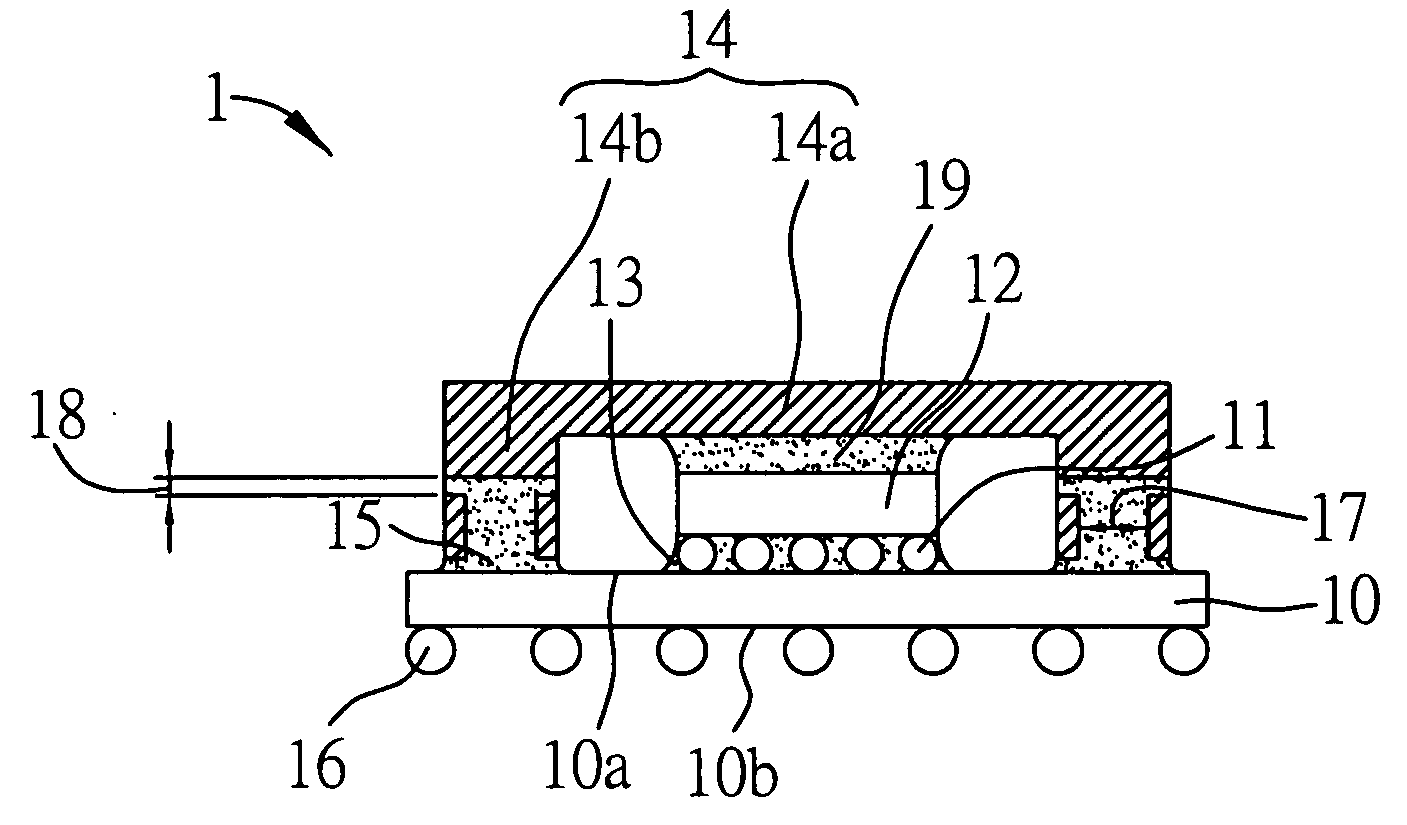
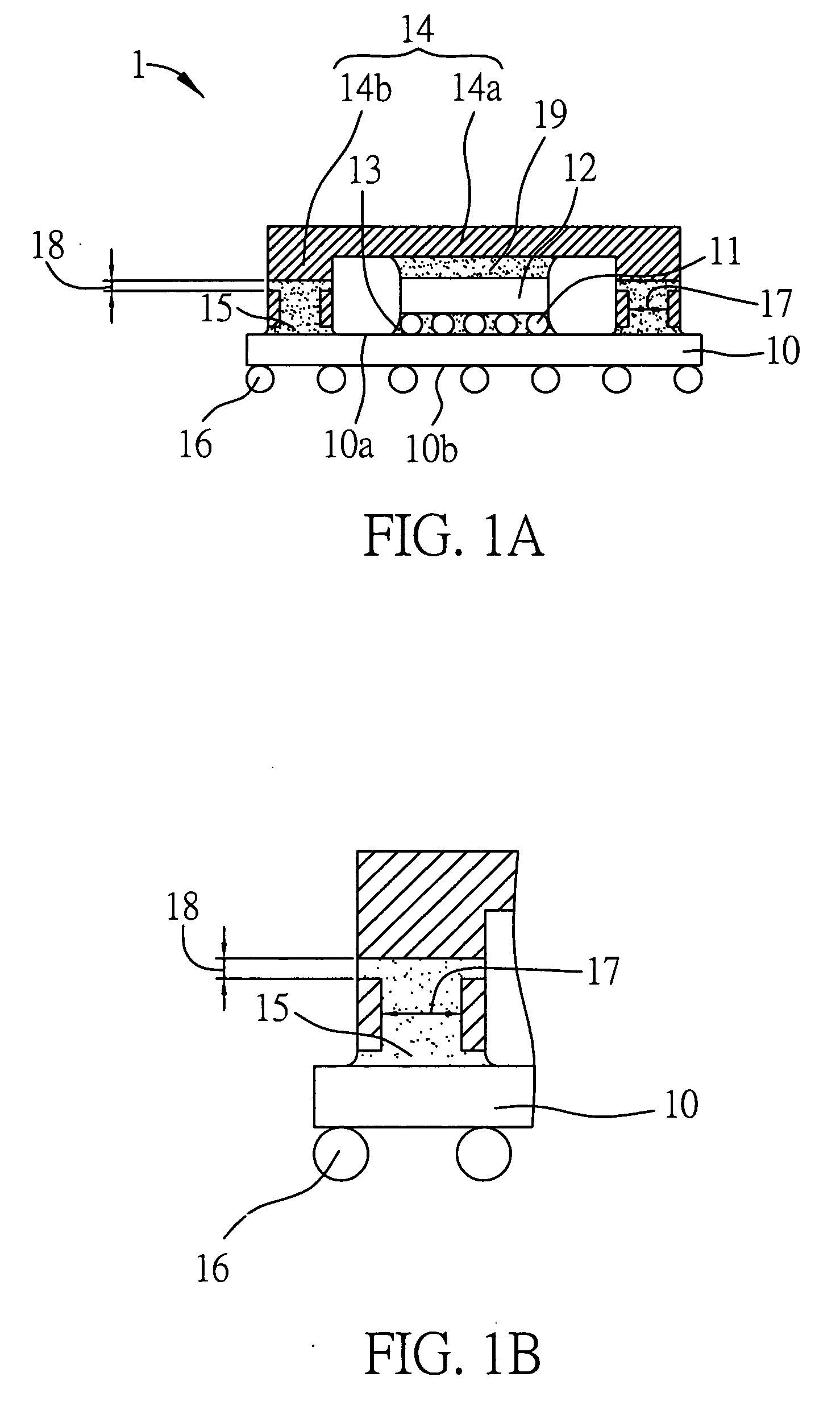
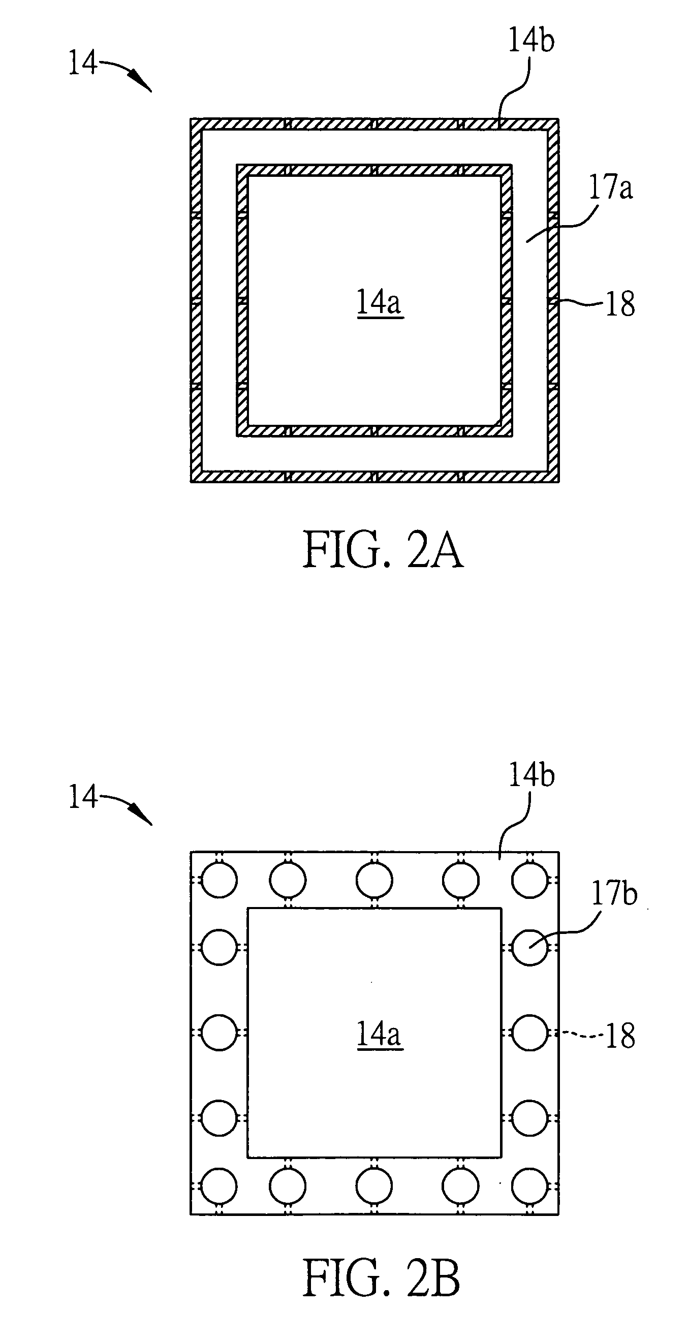
[0030] First, referring to FIG. 1A showing a cross-sectional view of a semiconductor package according to a preferred embodiment of the present invention, which is preferably a flip-chip ball grid array (FCBGA) package comprising: a substrate 10 used as a chip carrier; a semiconductor chip 12 mounted on a first surface 10a of the substrate 10 and electrically connected to the substrate 10 via a plurality of conductive bumps 11; an underfill insulating material 13 applied around the conductive bumps 11; a heat dissipating structure 14 mounted on the first surface 10a of the substrate 10; an adhesive 15 applied between the heat dissipating structure 14 and the first surface 10a of the substrate 10; and a plurality of solder balls 16 formed on a second surface 10b of the substrate 10 and electrically connected to the conductive bumps 11. The heat dissipating structure 14 comprises a flat portion 14a and a support portion 14b extending from the periphery of the flat portion 14a toward t...


PUM


Abstract

A heat dissipating structure and a semiconductor package with the same are proposed. A substrate is used to accommodate at least one chip thereon, and the chip is electrically connected to the substrate. A heat dissipating structure having a flat portion and a support portion is mount on the substrate via the support portion by means of an adhesive. At least one groove is formed on the support portion and at least one air vent is formed around the groove to allow the groove to communicate with the outside via the air vent, such that the adhesive is allowed to fill the groove to expel air from the groove to the atmosphere through the air vent, thereby preventing the air from trapped in the groove.

Description

FIELD OF THE INVENION [0001] The present invention relates to semiconductor packages, and more particularly, to a semiconductor package with a heat dissipating structure that can be firmly attached to a chip carrier so as to improve the adhesion reliability between the heat dissipating structure and the chip carrier. BACKGROUND OF THE INVENTION [0002] Flip-chip ball grid array (FCBGA) semiconductor package combines flip-chip and ball-grid-array structures, wherein at least one semiconductor chip is incorporated in a flip-chip manner that an active surface of the chip is electrically connected to a side of a substrate via a plurality of conductive bumps, and a plurality of solder balls are formed on an opposite side of the substrate to serve as input / output (I / O) connections. This FCBGA package desirably has a reduced size and improved electrical performance as not requiring the use of bonding wires, thereby reducing the resistance and preventing signal degradation during transmissio...

Claims


Application Information

Patent Timeline
Patent Type & Authority Applications(United States)
IPC IPC(8): H01L23/10H01L23/36
CPCH01L23/10H01L23/36H01L2924/16251H01L2224/73204H01L2224/32225H01L2224/16225H01L2224/73253H01L2924/15311H01L2924/16152H01L2924/163H01L2924/16315H01L2924/00
Inventor CHEN, CHIN-TELIN, CHANG-FU
Owner SILICONWARE PRECISION IND CO LTD
Why Eureka
Try Eureka