When the particle is small compared to the optical
point spread function of the lens and small compared to the digitizing pixel, the brightfield energy from the immediate areas surrounding the particle usually contribute a lot of energy, thus the very small reduction in returned energy due to the particle size makes the particle difficult to detect.
Further, the small reduction in energy from the
small particle is often masked out by
reflectivity variations of the bright surrounding background such that
small particles cannot be detected without a lot of false detections.
Also, if the
small particle is on an area of very low
reflectivity, which occurs for some process
layers on wafers and always for reticles, photomasks and
flat panel displays, the background return is already low thus a further reduction due to the presence of a particle is very difficult to detect.
While this works well for blank and unpatterned specimens, in the presence of circuit features it can only detect large particles which protrude above the circuit features.
The resulting detection sensitivity is not satisfactory for advanced VLSI circuit production.
The major limitation of spatial filtering based instruments is that they can only inspect areas with repeating patterns or blank areas.
That is a fundamental limitation of that technology.
As a result, either
small particles in the array areas cannot be seen due to saturation, or small particles in the
peripheral areas cannot be detected due to insufficient
signal strength.
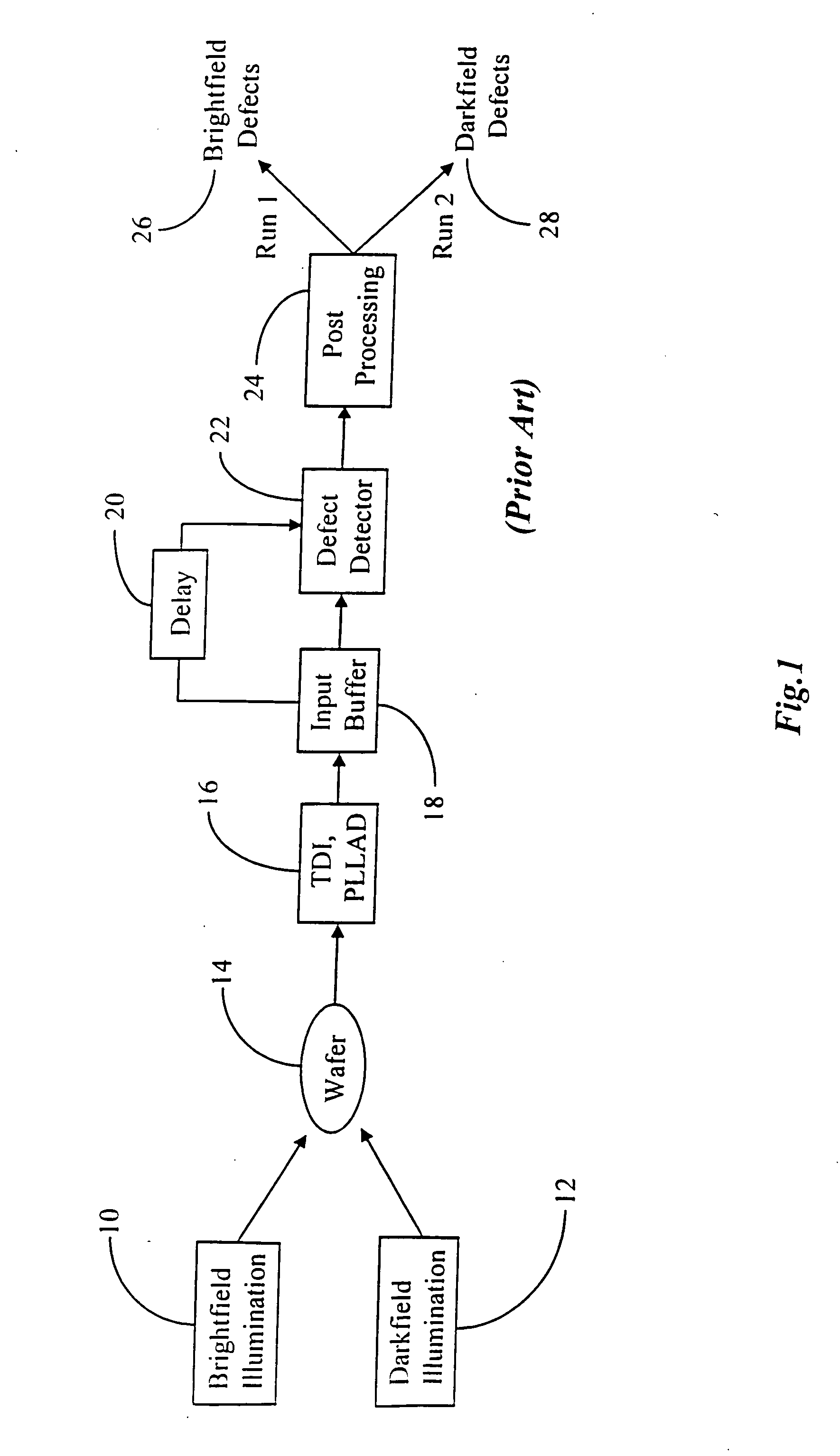
There are two major disadvantages to the Hitachi darkfield / spatial filtering / die-to-die inspection
machine.
Second, since the filtered images are usually dark without circuit features, it is not possible to do an accurate die-to-die
image alignment, which is necessary for achieving good cancellation in a subtraction
algorithm.
Hitachi's solution is to use an expensive mechanical stage of very high precision, but even with such a stage, due to the pattern placement variations on the wafer and residual errors of the stage, the achievable sensitivity is limited roughly to particles that are 0.5 μm and larger.
Other than the activity by Hitachi, Tencor Instruments (U.S. Pat. No. 5,276,498), OSI (U.S. Pat. No. 4,806,774) and IBM (U.S. Pat. No. 5,177,559), there has been no interest in a combination of brightfield and darkfield techniques due to a lack of understanding of the advantages presented by such a technique.
The conventional
microscope that has both brightfield and
darkfield illumination, has a single
light source that provides both illuminations simultaneously, thus making it impossible to separate the brightfield and darkfield results from each other.
In at least one commercially available
microscope from Zeiss it is possible to have separate brightfield and
darkfield illumination sources simultaneously, however, there is a single
detector and thus there is no way to separate the results of the brightfield and darkfield illumination from each other.

