Method of reading NAND memory to compensate for coupling between storage elements

a technology of nand memory and coupling, applied in the field of nonvolatile memory, can solve the problems of reducing the ability of designers to increase the speed and reliability of devices

Inactive Publication Date: 2005-07-28
SANDISK TECH LLC
View PDF24 Cites 286 Cited by
  • Summary
  • Abstract
  • Description
  • Claims
  • Application Information

AI Technical Summary

Benefits of technology

[0055] In word line WLn, it will be noted that because of the Yupin effect discussed above, the apparent distributions of the “11” and “10” (as shown by the broadening dashed lines states) becomes broader than the threshold distributions indicated by the solid lines that exist immediately after their programming. This is because the initial programming of data of word line WLn is done in an environment where no adjacent floating gates contain the higher charge levels that represent the “00” and “01” states. The broadening of the apparent initial distributions occurs when adjacent cells, such as cells in an adjacent word line WLn+1, are programmed to these higher threshold level states. Further, the higher states “00” and “01” also suffer this apparent broadening effect since adjacent floating gates are written with data.
[0056] The effect o

Problems solved by technology

The problem occurs most pronouncedly between two sets of adjacent cells that have been programmed at different times. One set of cells is programmed to add a level of charge to their floating gates that corresponds t

Method used


Image

  • Method of reading NAND memory to compensate for coupling between storage elements
  • Method of reading NAND memory to compensate for coupling between storage elements
  • Method of reading NAND memory to compensate for coupling between storage elements

Examples


Embodiment Construction

[0033] A method for reading a memory device which reduces the Yupin effect on adjacent cells is described herein. An exemplary memory device is discussed below and the method may be utilized on such device. However, the method may be performed on many other types of devices and is not limited to the particular device described herein.

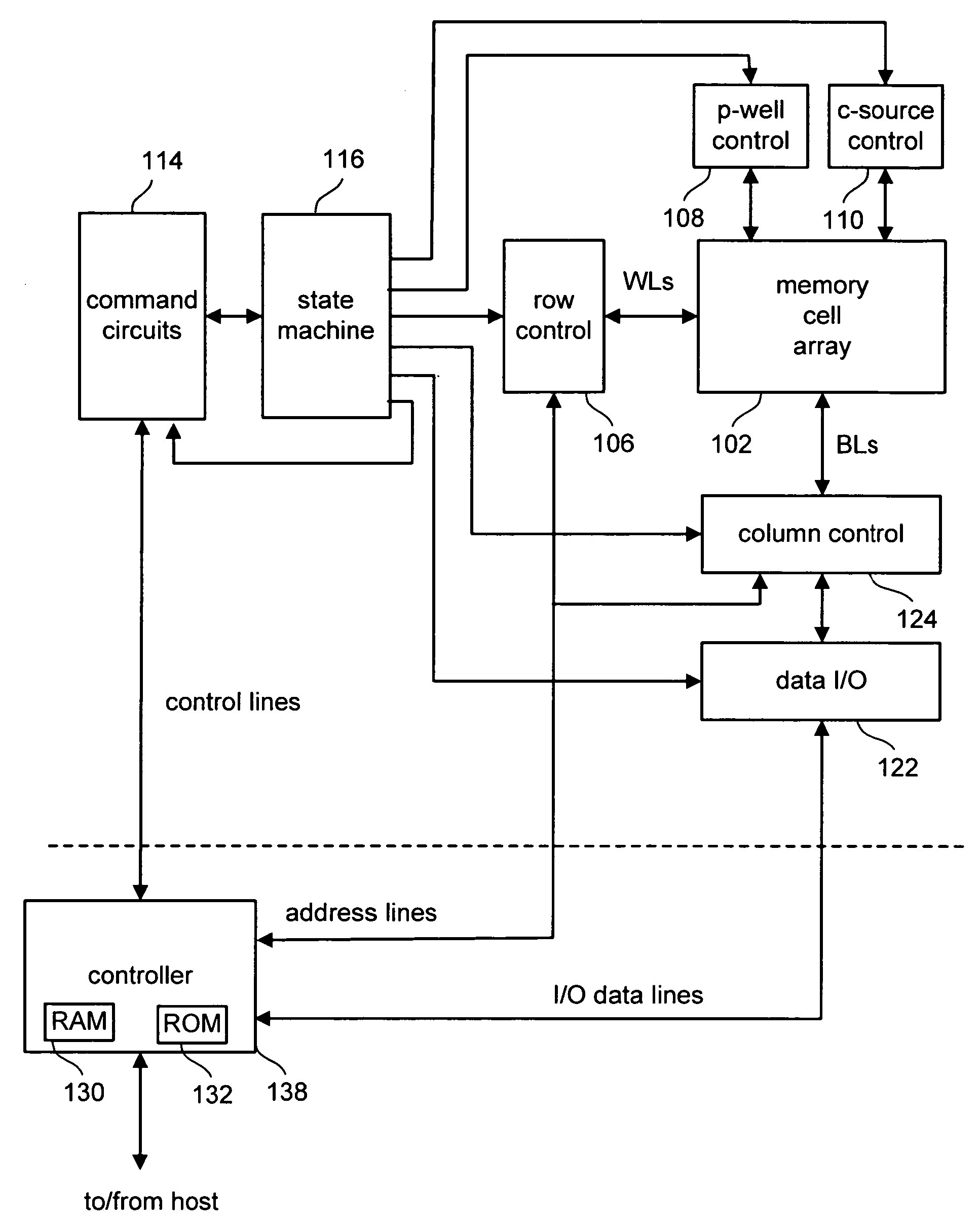
[0034]FIG. 1 is a block diagram of one embodiment of a flash memory system that can be used to implement the present invention. Memory cell array 102 is controlled by column control circuit 124, row control circuit 106, c-source control circuit 110 and p-well control circuit 108. Column control circuit 124 is connected to the bit lines of memory cell array 102 for reading data stored in the memory cells, for determining a state of the memory cells during a program operation, and for controlling potential levels of the bit lines to promote the programming or to inhibit the programming. Row control circuit 106 is connected to the word lines to select one...


PUM


Abstract

A method for reading non-volatile memory arranged in columns and rows which reduces adjacent cell coupling, sometimes referred to as the Yupin effect. The method includes the steps of: selecting a bit to be read in a word-line; reading an adjacent word line written after word line; and reading the selected bit in word line by selectively adjusting at least one read parameter. In one embodiment, the read parameter is the sense voltage. In another embodiment, the read parameter is the pre-charge voltage. In yet another embodiment, both the sense and the pre-charge voltage are adjusted.

Description

BACKGROUND OF THE INVENTION [0001] 1. Field of the Invention [0002] This invention relates generally to a non-volatile memory and its operation, and, more specifically, to techniques for reducing the effects of data stored in one memory storage element upon data read from other storage elements. [0003] 2. Description of the Related Art [0004] Electrical Erasable Programmable Read Only Memory (EEPROM) and flash memory are among the most popular non-volatile semiconductor memories. They are used in cellular telephones, digital cameras, personal digital assistants, mobile computing devices, non-mobile computing devices, desktop computers and other devices. [0005] Typical EEPROMs and flash memories utilize a memory cell with a floating gate that is provided above and insulated from a channel region in a semiconductor substrate. The floating gate is positioned above and between source and drain regions. A control gate is provided over and insulated from the floating gate. The threshold v...

Claims


Application Information

Patent Timeline
IPC IPC(8): G11C11/56G11C16/04G11C16/26H01L27/115
CPCG11C11/5642G11C16/0483H01L27/115G11C16/3418G11C16/3422G11C16/26H10B69/00G11C16/02G11C16/08G11C16/34
Inventor CHEN, JIAN
Owner SANDISK TECH LLC
Why Eureka
Try Eureka