Method of manufacturing a semiconductor device

Active Publication Date: 2005-07-28
SAMSUNG ELECTRONICS CO LTD
View PDF3 Cites 17 Cited by
  • Summary
  • Abstract
  • Description
  • Claims
  • Application Information

AI Technical Summary

Benefits of technology

[0025] Embodiments of the invention provide a method of manufacturing a semiconductor device that prevents the gate pattern from being broken while obtaining a sufficient processing margin for overlap with an active region.
[0026] Accord

Problems solved by technology

As a result, the transistors of the SRAM cannot be formed into a lined gate structure such as the gate structure of the cell of a DRAM or a non-volatile memory (NVM).

Method used


Image

  • Method of manufacturing a semiconductor device
  • Method of manufacturing a semiconductor device
  • Method of manufacturing a semiconductor device

Examples


Embodiment Construction

[0034] The teachings of the invention are described more fully below with reference to the accompanying drawings where exemplary embodiments of the invention are shown.

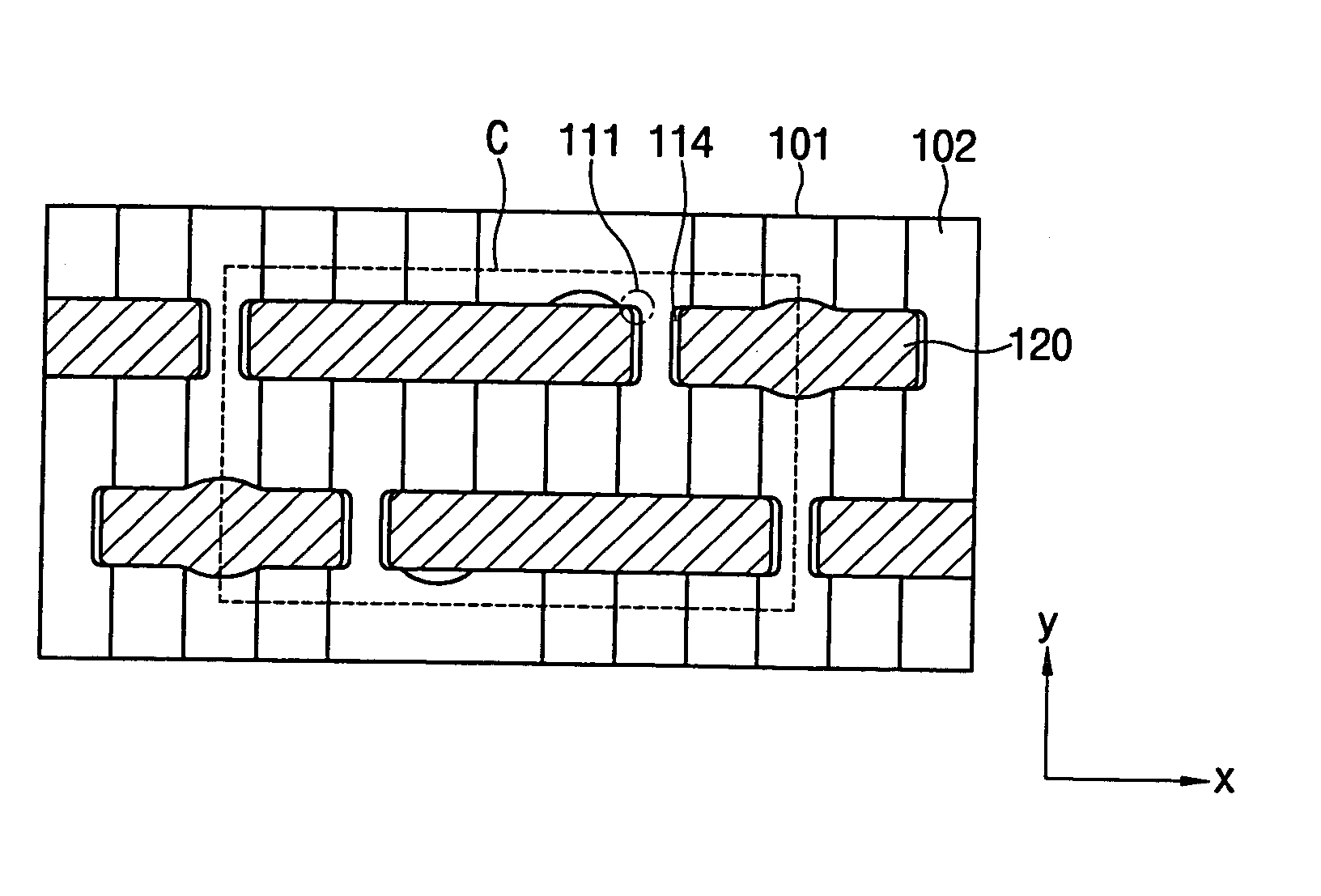
[0035]FIG. 4 is a plan view schematically illustrating an active region and a separated gate pattern in a cell of a full CMOS type SRAM according to some embodiments of the invention.

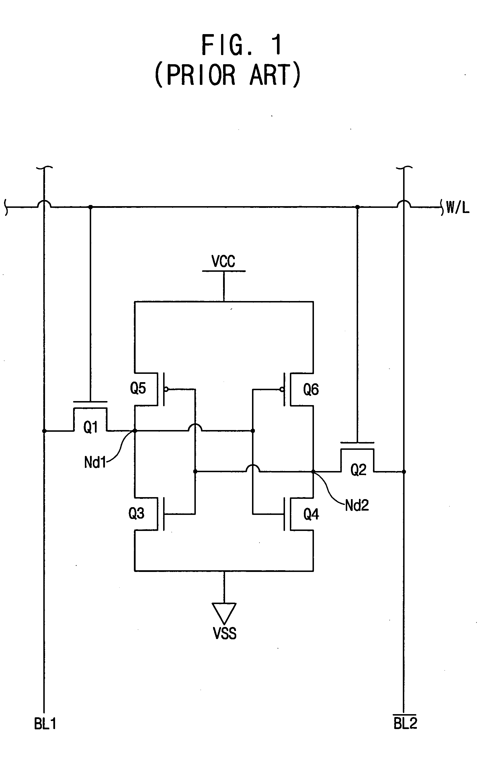
[0036] The cell structure of the full CMOS type SRAM according to some embodiments of the invention include the same components as that of the conventional full CMOS type SRAM as illustrated in FIG. 1.

[0037] That is, a cell of the full CMOS type SRAM according to some embodiments of the invention includes first and second pass transistors Q1 and Q2, a first P-MOS transistor Q5, and a first N-MOS transistor Q3. The first pass transistor Q1 electrically connects a first bit line BL1 with a first memory cell node Nd1, and the second pass transistor Q2 electrically connects a second bit line BL2 with a second memory cell node Nd2. The firs...


PUM


Abstract

In a method of manufacturing a semiconductor device including independent gate patterns separated from each other, an active region is defined by forming a field region on a substrate. A gate oxide layer and a polysilicon layer are formed on the substrate. A preliminary gate pattern is formed by partially removing the polysilicon layer along a first direction by a first etching process. A spacer is formed along a side surface of the preliminary gate pattern. A number of separated gate patterns is formed by partially removing the preliminary gate pattern along a second direction crossing the first direction by a second etching process. The gate patterns overlap with the active regions and are separated from each other. Therefore, the overlap margin is increased, and the polysilicon layer is prevented from being over-etched when it is patterned to form the gate pattern.

Description

CROSS-REFERENCE TO RELATED APPLICATIONS [0001] This application claims priority from Korean Patent Application No. 2003-76570 filed on Oct. 31, 2003, the content of which is herein incorporated by reference in its entirety for all purposes. BACKGROUND OF THE INVENTION [0002] 1. Field of the Invention [0003] This disclosure relates to a method of manufacturing a semiconductor device, and more particularly, to a method of manufacturing a semiconductor device having separated and independent gate patterns with minute thicknesses. [0004] 2. Description of the Related Art [0005] Generally, a semiconductor memory device is classified into dynamic random access memory (DRAM) and static random access memory (SRAM) in accordance with data storing method. An SRAM device has many advantages such as a high operating speed, low power consumption, and simplified operation, thus it has been the focus of intense interest in recent years. In addition, the SRAM device is also advantageous because no ...

Claims


Application Information

Patent Timeline
IPC IPC(8): H01L21/336H01L21/8244H01L27/11
CPCH01L27/1104H01L27/11H10B10/00H10B10/12
Inventor JANG, WOO-SOONKIM, JOONCHUNG, EUN-KUK
Owner SAMSUNG ELECTRONICS CO LTD
Why Eureka
Try Eureka