Laterally diffused metal oxide semiconductor device and method of forming the same

Inactive Publication Date: 2005-08-04
TAHOE RES LTD
View PDF54 Cites 123 Cited by
  • Summary
  • Abstract
  • Description
  • Claims
  • Application Information

AI Technical Summary

Benefits of technology

[0012] These and other problems are generally solved or circumvented, and technical advantages are generally achieved, by advantageous embodiments of the present invention which includes a transistor advantageously embodied in a laterally diffused metal oxide semiconductor (“LDMOS”) device having a gate located over a channel region recessed into a semiconductor substrate and a method of forming the same. In one embodiment, the LDMOS device includes a source/drain having a lightly doped region located adjacent the channel region and a heavily doped region located adjacent the lightly doped region. The LDMOS device further includes an oppositely doped well located under and within the channel region, and a doped region, located between the heavily doped region and the oppositely doped well, having a doping concentration profile less than a doping concentration profile of the heavily doped region. In one advantageous embodiment, the source/drain includes P-type lightly and heavily doped regions and the oppositely doped well is a N-type well. In accordance therewith, the doped region is a P-type doped region having a doping concentration profile less than a doping concentra

Problems solved by technology

An objective of incorporating control and signal processing devices on a semiconductor substrate with the higher voltage devices often encounters conflicting design requirements.
Since the cost of an integrated circuit is roughly proportional to the number of processing steps to construct the same, there has been limited progress in the introduction of low cost integrated circuits that include both control

Method used


Image

  • Laterally diffused metal oxide semiconductor device and method of forming the same
  • Laterally diffused metal oxide semiconductor device and method of forming the same
  • Laterally diffused metal oxide semiconductor device and method of forming the same

Examples


Embodiment Construction

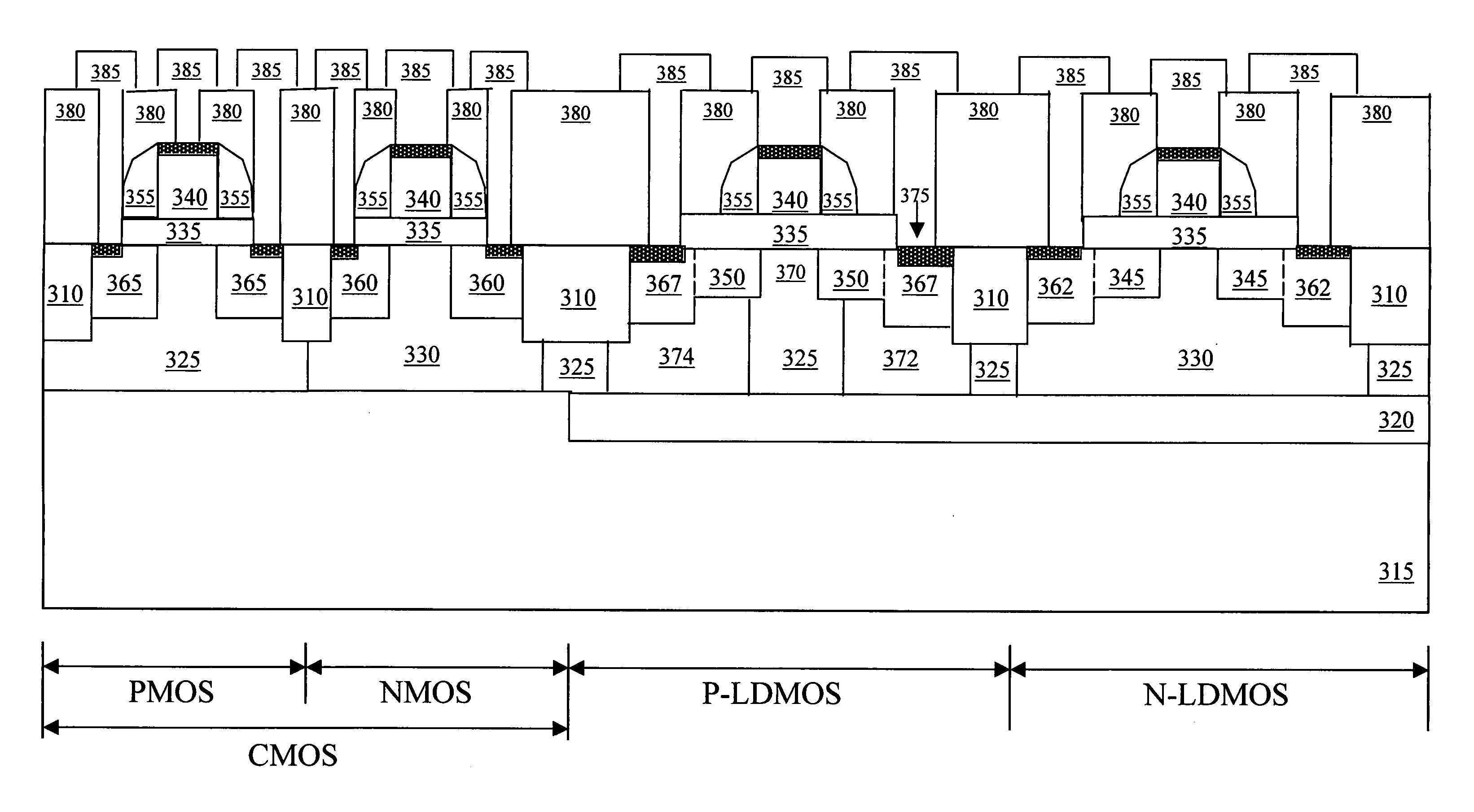
[0020] The making and using of the presently preferred embodiments are discussed in detail below. It should be appreciated, however, that the present invention provides many applicable inventive concepts that can be embodied in a wide variety of specific contexts. The specific embodiments discussed are merely illustrative of specific ways to make and use the invention, and do not limit the scope of the invention.

[0021] The present invention will be described with respect to preferred embodiments in a specific context, namely, a transistor [e.g., embodied in a laterally diffused metal oxide semiconductor (“LDMOS”) device], a semiconductor device incorporating the LDMOS device and methods of forming the same. While the principles of the present invention will be described in the environment of a power converter, any application that may benefit from a transistor that can accommodate higher voltages and is integrable with a low voltage device [e.g., complementary metal oxide semicondu...


PUM


Abstract

A transistor advantageously embodied in a laterally diffused metal oxide semiconductor device having a gate located over a channel region recessed into a semiconductor substrate and a method of forming the same. In one embodiment, the laterally diffused metal oxide semiconductor device includes a source/drain having a lightly doped region located adjacent the channel region and a heavily doped region located adjacent the lightly doped region. The laterally diffused metal oxide semiconductor device further includes an oppositely doped well located under and within the channel region, and a doped region, located between the heavily doped region and the oppositely doped well, having a doping concentration profile less than a doping concentration profile of the heavily doped region.

Description

TECHNICAL FIELD [0001] The present invention is directed, in general, to the semiconductor devices and, more specifically, to a laterally diffused metal oxide semiconductor device and method of forming the same. BACKGROUND [0002] The design of early integrated circuits focused on implementing an increasing number of small semiconductor devices on a semiconductor substrate to achieve substantial improvements in manufacturing efficiency and cost, product size, and performance. The continuing improvements in the design of integrated circuits over the past few decades has been so dramatic and so pervasive in numerous products that the effects can be measured in changes in industries. [0003] The design and construction of integrated circuits has continued to evolve in a number of different areas. One area of innovation is a continuing reduction of feature sizes of semiconductor devices such as control and signal processing devices formed on a semiconductor substrate. Another area of inno...

Claims


Application Information

Patent Timeline
IPC IPC(8): H01L21/336H01L21/761H01L21/8238
CPCH01L21/761H01L29/7816H01L21/823878H01L21/823892H01L29/0847H01L29/0878H01L29/1083H01L29/1095H01L29/456H01L29/4933H01L29/665H01L29/66659H01L29/66689H01L29/78H01L29/7833H01L27/0629H01L21/823814
Inventor LOTFI, ASHRAF W.TAN, JIAN
Owner TAHOE RES LTD
Why Eureka
Try Eureka