Semiconductor device and manufacturing method thereof
- Summary
- Abstract
- Description
- Claims
- Application Information
AI Technical Summary
Problems solved by technology
Method used
Image

Examples
first embodiment
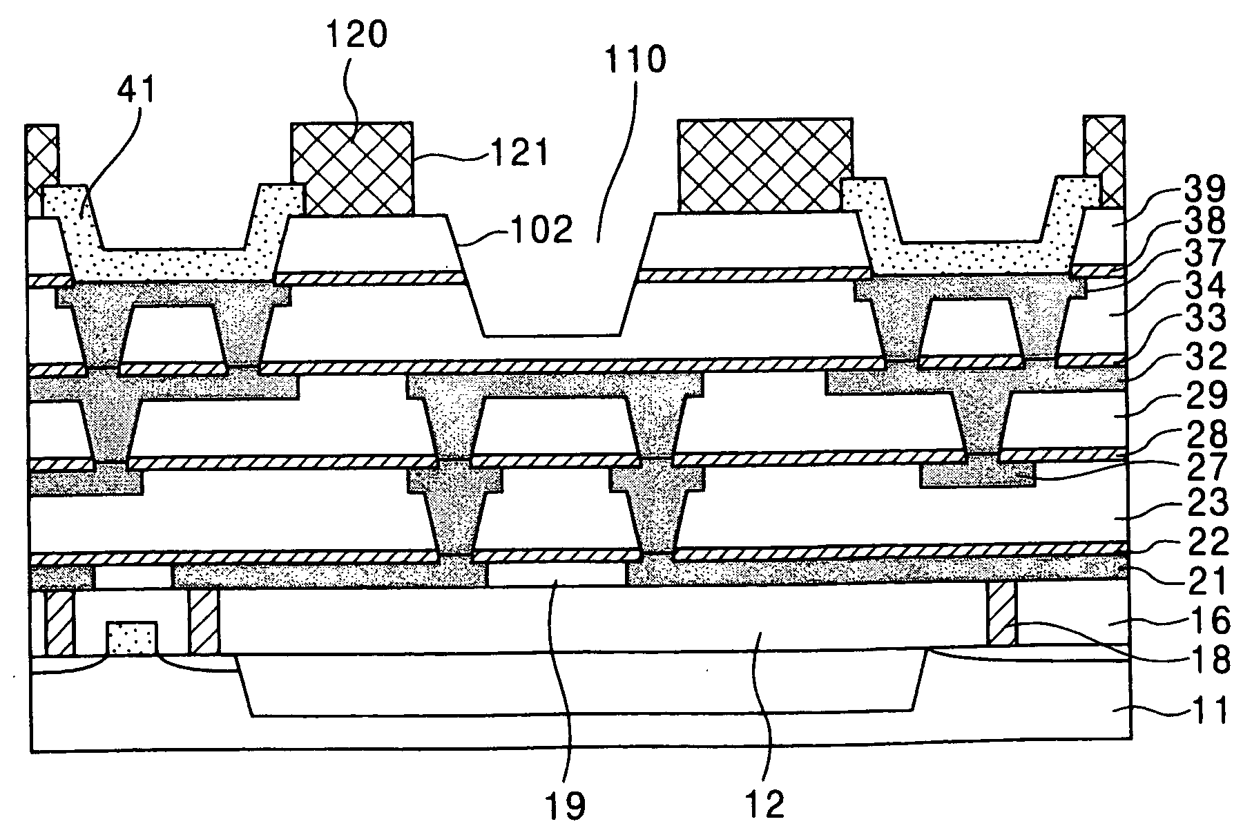
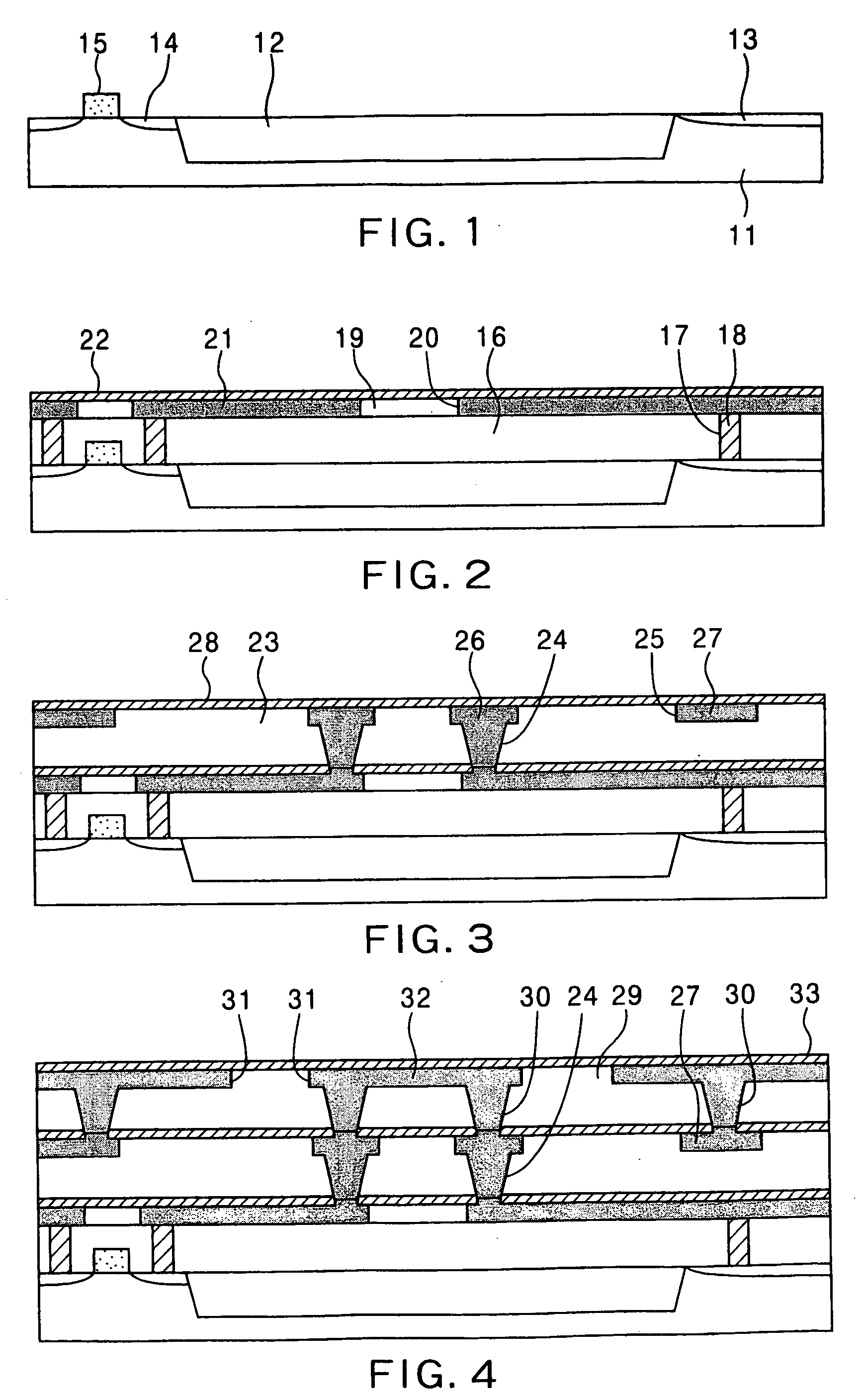
[0053] FIGS. 1 to 9 are cross section diagrams of process steps showing a manufacturing method of a semiconductor device according to the present invention.
[0054] At first, as shown in FIG. 1, a device isolation area 12 is formed in a surface part of a silicon substrate 11 using the ordinal Shallow Trench Isolation (STI) technology. Then, a diffusion region 13 which will be a passive device such as capacitor and an active elements such as MOSFET having a source and drain diffusion regions 14 and a gate 15 is formed in a device area which is surrounded by the device isolation region.
[0055] Then, as shown in FIG. 2, the first interlayer insulating film 16 such as BPSG film is deposited on the whole surface and the surface is flattened with CMP method. After that, a first contact hole 17 is opened with photo lithography method and a contact 18 is formed by filling the contact hole 17 with tungsten. Thereafter, a second interlayer insulating film 19 such as SiO2 film is deposited on th...
second embodiment
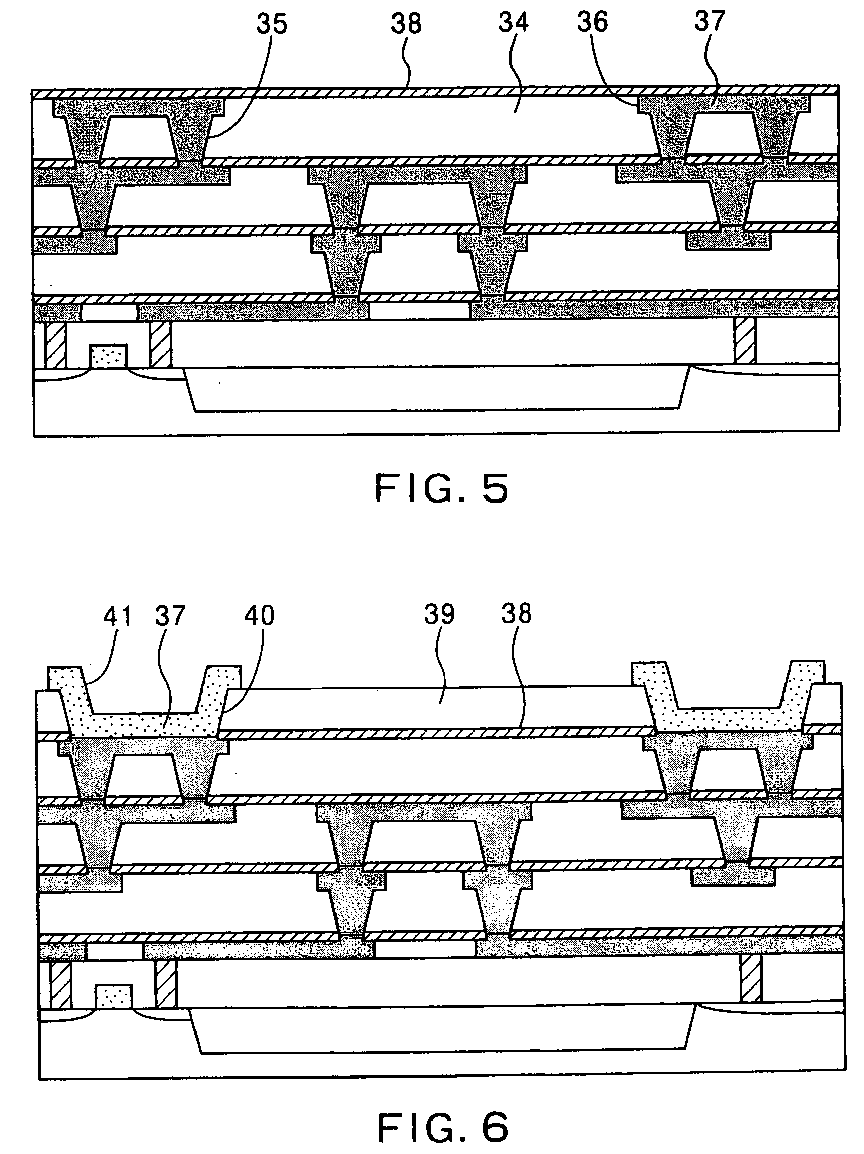
[0066] FIGS. 10 to 13 are cross section diagrams by process showing a manufacturing method of a semiconductor device according to the present invention.
[0067]FIG. 10 is exactly the same as FIG. 5 according to the first embodiment of the invention. In the following description, common reference numbers are used for the same elements between them.
[0068] As shown in FIG. 11, a passivation film 60 such as PSG film is deposited and the passivation film on the fourth interconnection layer 37 to be a bonding pad and the passivation film at the fuse window opening 70 are etched with photo lithography method to form openings 61 and 62 respectively. At this time, the thin silicon nitride film 38 is also etched at the area, the fourth copper interconnection 37 is exposed at the bonding pad forming area and the a part 63 of the surface of the fifth interlayer insulating film 34 is etched at the fuse window opening.
[0069] After that, a bonding pad 63 is formed by depositing aluminum and reserv...
PUM
 Abstract
Description
Claims
Application Information
PatSnap Eureka turns technology decisions into work you can execute. Powered by our Innovation Knowledge Graph, it runs expert workflows across engineering, life sciences, materials and intellectual property. Get your review-ready output in minutes.


