Field emission backlight device

a backlight device and field technology, applied in the field of field emission backlight devices, can solve the problems of high production cost and high light loss of plate-type backlight devices, and achieve the effect of improving luminance uniformity

Inactive Publication Date: 2005-08-11
SAMSUNG SDI CO LTD
View PDF9 Cites 27 Cited by
  • Summary
  • Abstract
  • Description
  • Claims
  • Application Information

AI Technical Summary

Benefits of technology

[0011] The present invention provides a field emission backlight device having an improv

Problems solved by technology

Such plate-type backlight devices have high production costs due to the use of the diffuser.
Further

Method used


Image

  • Field emission backlight device
  • Field emission backlight device
  • Field emission backlight device

Examples


Embodiment Construction

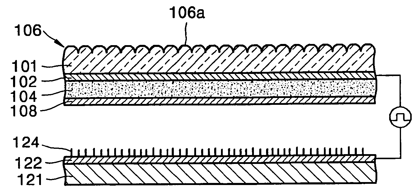
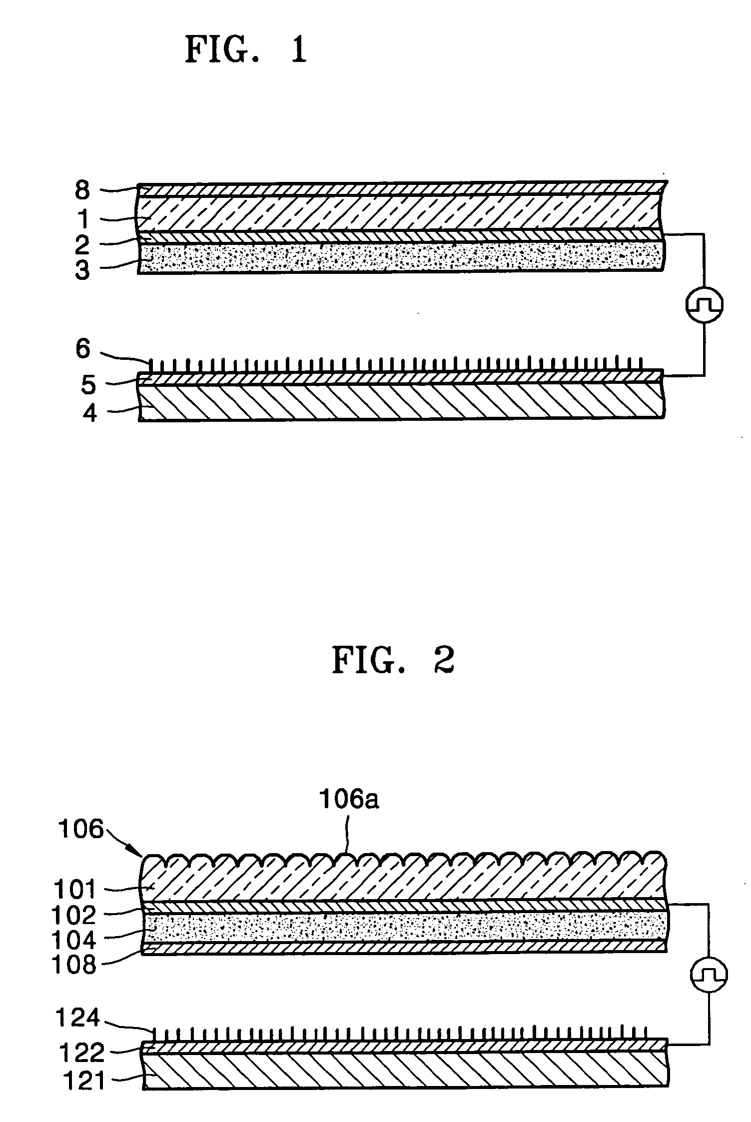
[0030]FIG. 1 is a schematic cross-sectional view illustrating the structure of a backlight device.

[0031] Referring to FIG. 1, spacers (not shown) are provided between a front substrate 1 and a rear substrate 4, and walls (not shown) between the front substrate 1 and the rear substrate 4 are sealed. A cathode 5 is provided in the form of a plate or a stripe on the rear substrate 4, and electron emitters 6, for example, made of Carbon NanoTubes (CNTs) are formed on the cathode 5. An anode 2, which is a transparent electrode, is formed on the front substrate 1 and a fluorescent layer 3 is coated on the anode 2.

[0032] A diffuser 8 is provided to overcome the problem that the light which passes through the front substrate 1 is not uniform.

[0033] When a predetermined voltage is supplied between the cathode 5 and the anode 2, electrons are emitted from the electron emitters 6 to excite the fluorescent layer 3. The light generated from the fluorescent layer 3 enters an LCD through the fl...


PUM


Abstract

A field emission backlight device includes: a front substrate and a rear substrate arranged in parallel and spaced apart from each other by a predetermined distance; an anode and a cathode arranged opposite to each other on a respective inner surfaces of the front and rear substrates; a fluorescent layer arranged on the anode and having a predetermined thickness; a convex portion including a plurality of convex projections arranged on an outer surface of the front substrate opposite to the anode; and electron emitters arranged on the cathode to emit electrons in response to an applied field.

Description

CLAIM OF PRIORITY [0001] This application makes reference to, incorporates the same herein, and claims all benefits accruing under 35 U.S.C. §119 from an application for FIELD EMISSION BACKLIGHT DEVICE earlier filed in the Korean Intellectual Property Office on 5 Feb. 2005 and there duly assigned Serial No. 2004-7526. BACKGROUND OF THE INVENTION [0002] 1. Field of the Invention [0003] The present invention relates to a field emission backlight device and method of manufacture thereof, and more particularly, to a field emission backlight device useful in Liquid Crystal Displays (LCDs) and a method of manufacture thereof. [0004] 2. Description of the Related Art [0005] Liquid crystal displays (LCDs) include backlight devices to generate white light on the back side thereof. In the past, cold cathode fluorescence lamps were used as backlight devices. However, backlight devices in the form of a plate were needed to provide thinner backlight devices. [0006] In a backlight device, spacers...

Claims


Application Information

Patent Timeline
IPC IPC(8): F21S2/00F21Y105/00G02F1/13357H01J29/89H01J63/06
CPCG02F1/133604G02F2001/133607H01J63/06H01J29/89G02F2001/133625G02F1/133607G02F1/133625G02F1/1335H01J1/30B82Y40/00
Inventor JUNG, JAE-EUNKIM, JONG-MINPARK, YOUNG-JUNLEE, HANG-WOO
Owner SAMSUNG SDI CO LTD
Why Eureka
Try Eureka