Liquid crystal display and manufacturing method for the same

a liquid crystal display and manufacturing method technology, applied in non-linear optics, instruments, optics, etc., can solve the problems of limiting the luminance of the display, the display itself darkening, and the manufacturing cost can be expensive, so as to achieve the effect of improving the efficiency of light usage and 100% aperture ratio

Inactive Publication Date: 2005-08-11
ILJIN DIAMOND
View PDF2 Cites 6 Cited by
  • Summary
  • Abstract
  • Description
  • Claims
  • Application Information

AI Technical Summary

Benefits of technology

[0020] The present invention makes aperture ratio 100% achieved and efficiency in light usage is improved, and forms lens on at least part of opposite substrate corresponding to wiring unit which cuts off light and then change path of light which is incident to wiring unit.

Problems solved by technology

However, the wider an area of the light cut-off unit gets, the smaller a corresponding aperture ratio gets, causing display itself to darken.
As a result, there is a limit to improve screen luminance.
According to the above manufacturing method, a manufacturing cost can be expensive because of a complicated manufacturing process.
In addition, since the process is performed from the opposite substrate-resin-cover glass in order, a sawing process only with a high cost in a cutting process can be usable.
In a prior micro lens manufacturing process, the cover glass should be attached in order to adjust the focal distance of the lenses and polished in regular thickness, thereby requiring a complicated process.
As a result, problems of the process and the manufacturing cost were serious due to such prior structure and the process.

Method used


Image

  • Liquid crystal display and manufacturing method for the same
  • Liquid crystal display and manufacturing method for the same
  • Liquid crystal display and manufacturing method for the same

Examples


Embodiment Construction

[0060] The present invention will now be described more fully hereinafter with reference to the accompanying drawings, in which preferred embodiments of the invention are shown.

[0061]FIG. 3a through FIG. 3f are diagrams illustrating a manufacturing process of an upper substrate used in a liquid crystal display panel in accordance with the present invention. Referring to FIG. 3a through FIG. 3f, the process will be described as follows.

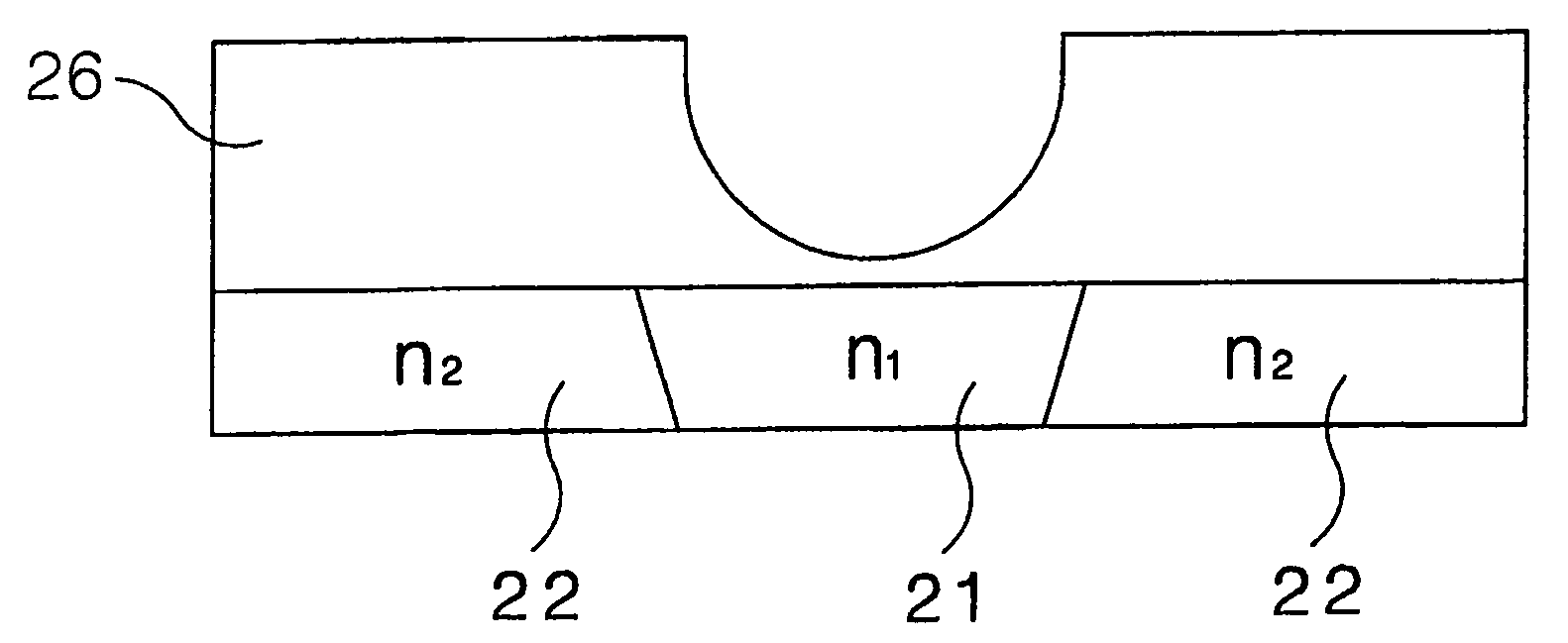
[0062] n2 thin films(12) having certain intervals are formed on many transparent substrates by being deposited and patterned on the transparent substrates. Then, an n1 thin film(11) is formed between the n2 thin films(12). At this time, the n2 thin films(12) can be formed in lamination shape of thin films whose stress is crossed in + and − directions. A location where the n1 thin film(11) is formed corresponds to a part where a light cut-off area of a lower substrate in the liquid crystal display panel is located (FIG. 3a).

[0063] A photoregister(16)...


PUM

PropertyMeasurementUnit
refractive indexaaaaaaaaaa
transparentaaaaaaaaaa
densityaaaaaaaaaa

Abstract

The present invention is related in upper glass, liquid crystal display panel, liquid crystal projector and method for liquid crystal display panel, more specifically, upper glass which is entering light is improved a ratio for aperture using semiconductor etching process. According to the present invention comprises transparent substrate which is transparent light; first thin film which is opposite opaque area on lower substrate make said transparent substrate; second thin film which is making around said first thin film on transparent substrate and thick film is equal density for said second thin layer and make on the said first thin film and said second thin film.

Description

TECHNICAL FIELD [0001] The present invention relates to an upper substrate, liquid crystal display panel, liquid crystal projector, and manufacturing method for the same, and more specifically, to an upper substrate, liquid crystal display panel, liquid crystal projector, and manufacturing method for the same for increasing an aperture ratio by directly forming a lens on the upper substrate on which light of the liquid crystal display panel is incident, through the application of a semiconductor etching process without a process of attaching another micro lens array. BACKGROUND ART [0002] An aperture ratio of a display element such as a liquid crystal display panel is a very important factor to determine performance, and shows degrees of light that is transmitted in the liquid crystal display panel. Since a display element having a high aperture ratio has a wider area for passing the light, the display element can be more brightly displayed than a display element having a low apertu...

Claims


Application Information

Patent Timeline
Patent Type & Authority Applications(United States)
IPC IPC(8): G02F1/1335
CPCG02F1/133526G02F1/1335
Inventor YUH, JINTAEBAE, BYUNGSEONG
Owner ILJIN DIAMOND
Why Eureka
Try Eureka