Packaged acoustic and electromagnetic transducer chips

a technology of electromagnetic transducer and acoustic wave, applied in the field of microstructure elements, can solve the problems of inability to manufacture and package chips, difficulty in packaging of mems microphones and other devices that require cavities, and inability to meet the requirements of the devi

Inactive Publication Date: 2005-09-01
TESSERA INC
View PDF99 Cites 200 Cited by
  • Summary
  • Abstract
  • Description
  • Claims
  • Application Information

AI Technical Summary

Problems solved by technology

The packaging of MEMS microphones and other devices that require cavities poses challenges.
One of the more challenging aspects of constructing such packages is to provide an interior cavity that exhibits the qualities required by a device, such as the acoustic cavity used in a package containing a microphone.
One of the challenges today is to provide an improved packaging technology that mates with smaller size microphone chips, thereby achieving reductions in the cost of fabricating and packaging chips.
However, if one needed to mount the packaged chip 60 instead in a different orientation which faces away from the circuit board 65, this would not be possible, because of the lack of conductive interconnects provided on the exterior bottom side 72 of the packaged chip.
However, image transducer chips are subject to being easily contaminated.
A particular challenge of packaging image transducer chips is mismatch between the coefficient of thermal expansion (CTE) of the chip, and the transparent material that covers the opening of a packaged image transducer chip.

Method used


Image

  • Packaged acoustic and electromagnetic transducer chips
  • Packaged acoustic and electromagnetic transducer chips
  • Packaged acoustic and electromagnetic transducer chips

Examples


Embodiment Construction

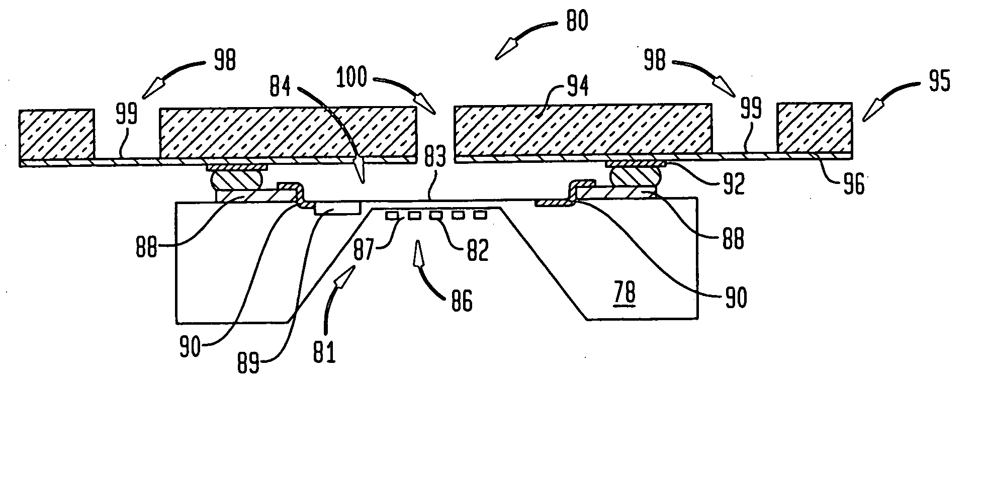
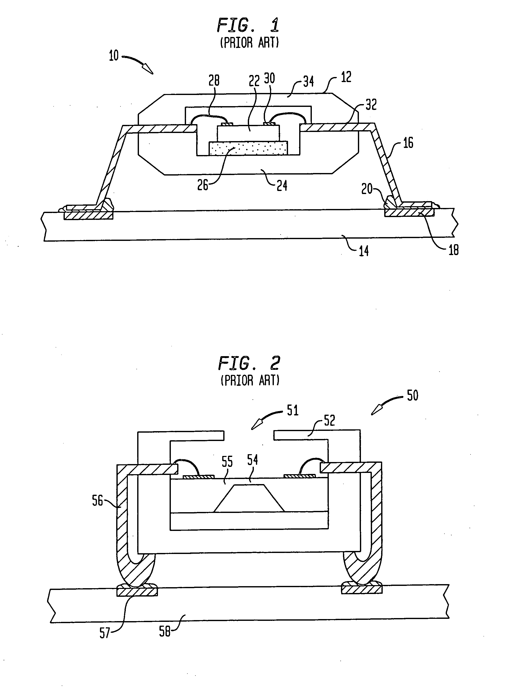
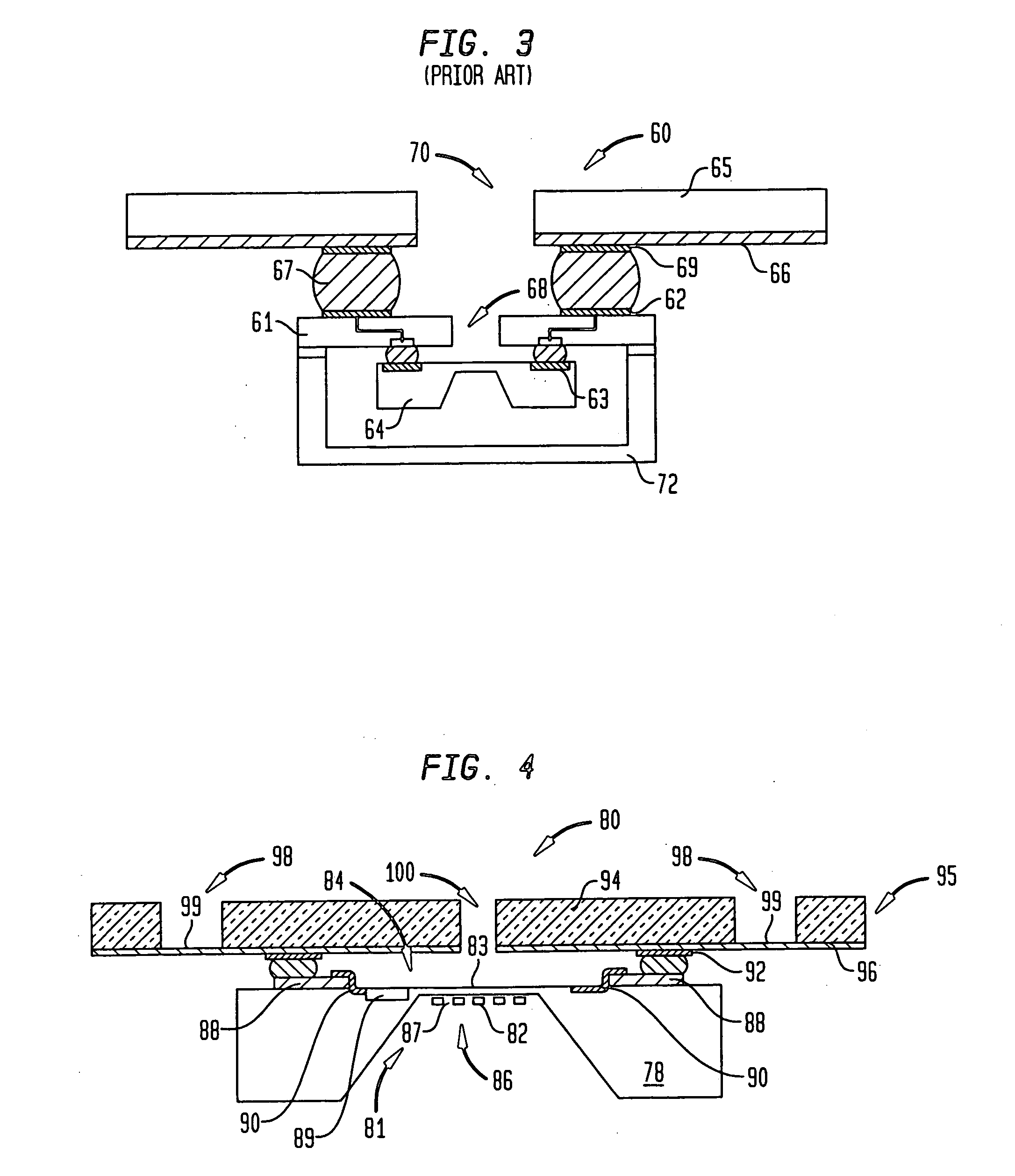
[0076] Microelectronic elements such as semiconductor chips or “dies” are commonly provided in packages which protect the die or other element from physical damage, and which facilitate mounting of the die on a circuit panel or other element. One type of microelectronic package includes a substrate, also referred to as a “tape” incorporating a dielectric layer such as a layer of a polyimide, BT resin or other polymeric material with electrically conductive features such as contacts on the dielectric element. The die is mounted on the substrate so that a face of the die confronts the substrate, typically with a layer of a die attach adhesive between the die and the substrate. The contacts or “terminals” are exposed at an outer surface of the substrate, but are electrically connected to contacts on the die itself. A protective material commonly referred to as an overmolding may surround the die itself, but desirably does not cover the terminals. Such a package can be mounted on a circ...


PUM


Abstract

Various embodiments of packaged chips and ways of fabricating them are disclosed herein. One such packaged chip disclosed herein includes a chip having a front face, a rear face opposite the front face, and a device at one of the front and rear faces, the device being operable as a transducer of at least one of acoustic energy and electromagnetic energy, and the chip including a plurality of bond pads exposed at one of the front and rear faces. The packaged chip includes a package element having a dielectric element and a metal layer disposed on the dielectric element, the package element having an inner surface facing the chip and an outer surface facing away from the chip. The metal layer includes a plurality of contacts exposed at at least one of the inner and outer surfaces, the contacts conductively connected to the bond pads. The metal layer further includes a first opening for passage of the at least one of acoustic energy and electromagnetic energy in a direction of at least one of to said device and from said device.

Description

CROSS-REFERENCE TO RELATED APPLICATIONS [0001] This application claims the benefit of the filing dates of U.S. Provisional Patent Application Nos. 60 / 549,176 filed Mar. 1, 2004; 60 / 561,210 filed Apr. 9, 2004; 60 / 568,041 filed May 4, 2004; and 60 / 574,523 filed May 26, 2004, the disclosures of all such applications being hereby incorporated herein by reference.BACKGROUND OF THE INVENTION [0002] The present invention relates to the packaging of microstructure elements such as integrated circuit chips, micro-electromechanical device chips and other types of chips. [0003] Certain types of chips require packaging that is open to the transmission of energy to and / or from outside the package. A microphone is one example. A microphone is a transducing device that converts acoustic pressure waves into electrical form. There exist many different types of microphones. One of the more common designs, favored on account of its combination of sensitivity, small physical dimensions and low power co...

Claims


Application Information

Patent Timeline
Patent Type & Authority Applications(United States)
IPC IPC(8): B81B7/00H01L23/495H04R19/00H04R19/04
CPCB81B7/0077B81B2201/0257H01L2924/07811H01L2224/48227H01L2924/12041H01L2224/16H01L2224/48228H01L2924/01078H01L2924/01079H01L2924/09701H01L2924/19041H01L2924/3025H04R19/005H01L2924/01019H01L2924/01087H01L2924/01322H01L2924/10253H01L2924/00H01L2924/10155H01L2224/05024H01L2224/05008H01L2224/05026H01L2224/05568H01L2224/05001H01L2224/05624H01L2224/73265H01L2924/10158H01L24/05H01L2924/00014
Inventor HUMPSTON, GILESOSBORN, PHILIP R.THOMPSON, JESSE BURLKUBOTA, YOICHITSENG, CHUNG-CHUANBURTZLAFF, ROBERTHABA, BELGACEMTUCKERMAN, DAVID B.WARNER, MICHAEL
Owner TESSERA INC
Why Eureka
Try Eureka