Nevertheless, problems with the long-term
image quality of these displays have prevented their widespread usage.
For example, particles that make up electrophoretic displays tend to settle, resulting in inadequate service-life for these displays.
Such gas-based electrophoretic media appear to be susceptible to the same types of problems due to particle
settling as liquid-based electrophoretic media, when the media are used in an orientation which permits such
settling, for example in a sign where the medium is disposed in a
vertical plane.
Indeed, particle
settling appears to be a more serious problem in gas-based electrophoretic media than in liquid-based ones, since the lower
viscosity of gaseous suspending fluids as compared with liquid ones allows more rapid settling of the electrophoretic particles.
However, vacuum lamination of the two parts of an electro-optic display in this manner imposes stringent requirements upon the lamination adhesive used, especially in the case of a display using an encapsulated electrophoretic medium.
The lamination adhesive must have adequate flow properties at the lamination temperature to ensure high quality lamination, and in this regard, the demands of laminating encapsulated electrophoretic and some other types of electro-optic media are unusually difficult; the lamination has be conducted at a temperature of not more than about 110° C. since the medium cannot be exposed to substantially higher temperatures without damage, but the flow of the adhesive must cope with the relatively uneven surface of the
capsule-containing layer, the surface of which is rendered irregular by the underlying capsules.
The lamination temperature should indeed be kept as low as possible, and
room temperature lamination would be ideal, but no commercial adhesive has been found which permits such
room temperature lamination.
As discussed in detail in the aforementioned U.S. Pat. No. 6,831,769, a lamination adhesive used in an electro-optic display must meet certain electrical criteria, and this introduces considerable problems in the selection of the lamination adhesive.
However, in such applications, the electrical properties of the lamination adhesive are not relevant, and consequently the commercial manufacturers pay no heed to such electrical properties.
If the resistivity of the adhesive layer is too high, a substantial
voltage drop will occur within the adhesive layer, requiring an increase in
voltage across the electrodes.
Increasing the
voltage across the electrodes in this manner is undesirable, since it increases the
power consumption of the display, and may require the use of more complex and expensive control circuitry to
handle the increased voltage involved.
On the other hand, if the adhesive layer, which extends continuously across the display, is in contact with a matrix of electrodes, as in an
active matrix display, the volume resistivity of the adhesive layer should not be too low, or lateral conduction of
electric current through the continuous adhesive layer may cause undesirable cross-talk between adjacent electrodes.
However, as the
conductivity of the lamination adhesive is increased at constant pixel resolution and storage
capacitance, charge supplied to a pixel is leaked to neighboring pixels; this decreases the
voltage gradient across the ink and counteracts the effect of increasing the lamination adhesive
conductivity.
In addition, as already mentioned this lateral charge leakage may cause a change in the optical state of neighboring pixels.
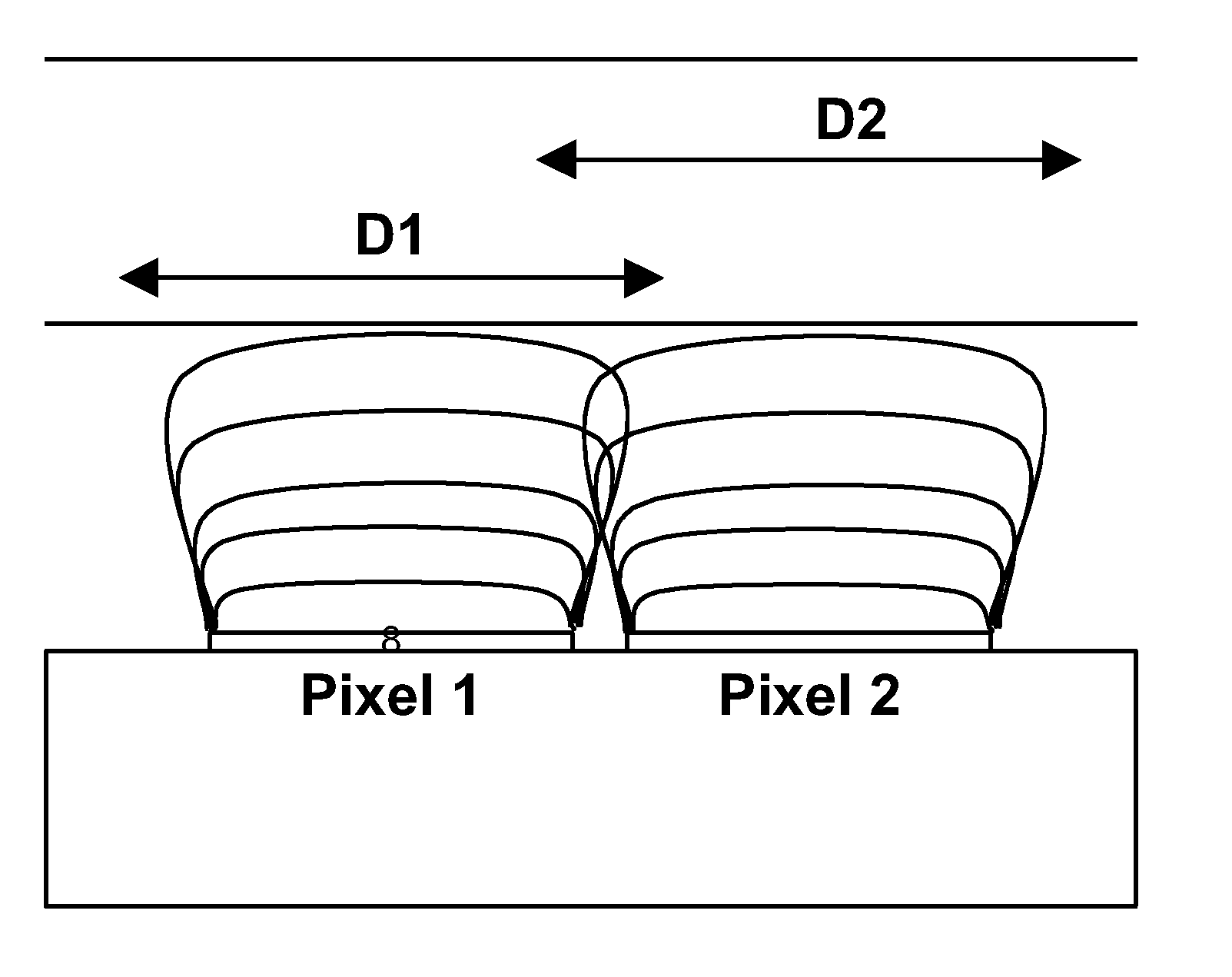
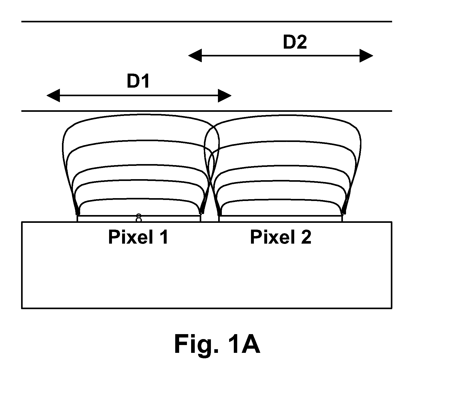
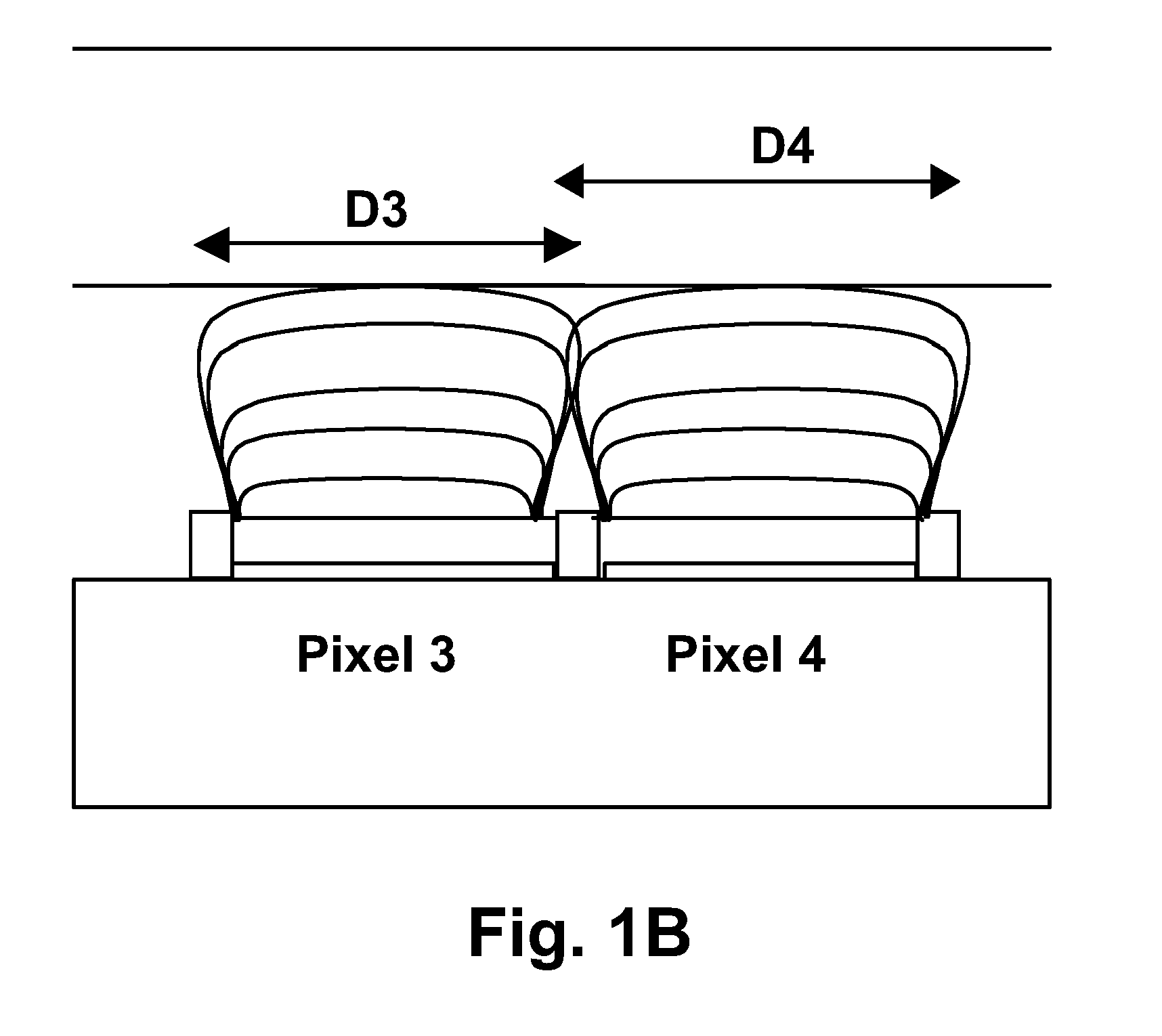
There is another problem associated with the use of adhesives in electro-optic displays, namely pixel “blooming”, that is to say the tendency for a pixel
electrode to cause a change in the display state of the electro-optic medium over an area larger than that occupied by the pixel
electrode itself.
Such pixel blooming is undesirable, since it adversely affects the quality of the displayed image.
Pixel blooming can be reduced by reducing the thickness of the adhesive layer, but an adhesive layer which is too thin may give rise to other problems.
An adhesive layer which is too thin may fail to provide sufficient adhesion and may also fail to planarize the
capsule layer.
Hence, it is not desirable to reduce the thickness of the adhesive layer too far, and the thickness chosen may be a compromise between that needed to reduce pixel blooming and that required for planarization and good adhesion.
However, the blooming should not be so great that the image intended to be displayed becomes distorted.

