Electroluminescence element

a technology of electroluminescent elements and el elements, which is applied in the field of electroluminescent elements, can solve the problems of non-uniform brightness of the light emission zone of the organic el element, relative great difference between the current densities of the corresponding portions of the organic light emission layer, and similar problems in the inorganic field, and achieves higher volume resistivity, lower volume resistivity, and high volume resistivity

Inactive Publication Date: 2006-09-28
TOYOTA IND CORP
View PDF4 Cites 11 Cited by
  • Summary
  • Abstract
  • Description
  • Claims
  • Application Information

AI Technical Summary

Benefits of technology

[0009] To achieve the above objective, the present invention provides an electroluminescence element including a first electrode, a second electrode, and a light emission layer arranged between the first and second electrodes. The first electrode is formed of a material having a higher volume resistivity than that of the material of the second electrode. A connector portion electrically connects a feeder portion to the first electrode. The resistance value of the connector portion differs in correspondence with a position at which the connector portion connects the feeder portion to the first electrode.
[0010] The present invention also provides an electroluminescence element including a first conductive layer, a light emission layer deposited on the first conductive layer, and a second conductive layer formed on the light emission layer. The first conductive layer has a terminal portion that can be connected to an external driver circuit. The first conductive layer is formed of a material having a higher volume resistivity than that of the material of the second conductive layer. An auxiliary electrode layer is provided in correspondence with a portion of the first conductive layer. The auxiliary electrode layer is formed of a material having a lower volume resistivity than that of the material of the first conductive layer. A high resistance portion is formed of a material having a higher volume resistivity than that of the material of the first conductive layer. The high resistance portion is arranged between the first conductive layer and the auxiliary electrode layer and adjacent to a portion of the light emission layer, extending along a side of the light emission layer. The high resistance portion has a length defined along a direction in which the side of the light emission layer extends and a width perpendicular to the length. The width of the high resistance portion differs in correspondence with the distance between the high resistance portion and the terminal portion.

Problems solved by technology

This results in a relatively great difference between the current densities of the corresponding portions of the organic light emission layer.
Accordingly, the brightness of the light emission zone of the organic EL element may become non-uniform.
Similar problems occur also in inorganic EL elements.

Method used


Image

  • Electroluminescence element
  • Electroluminescence element
  • Electroluminescence element

Examples


first embodiment

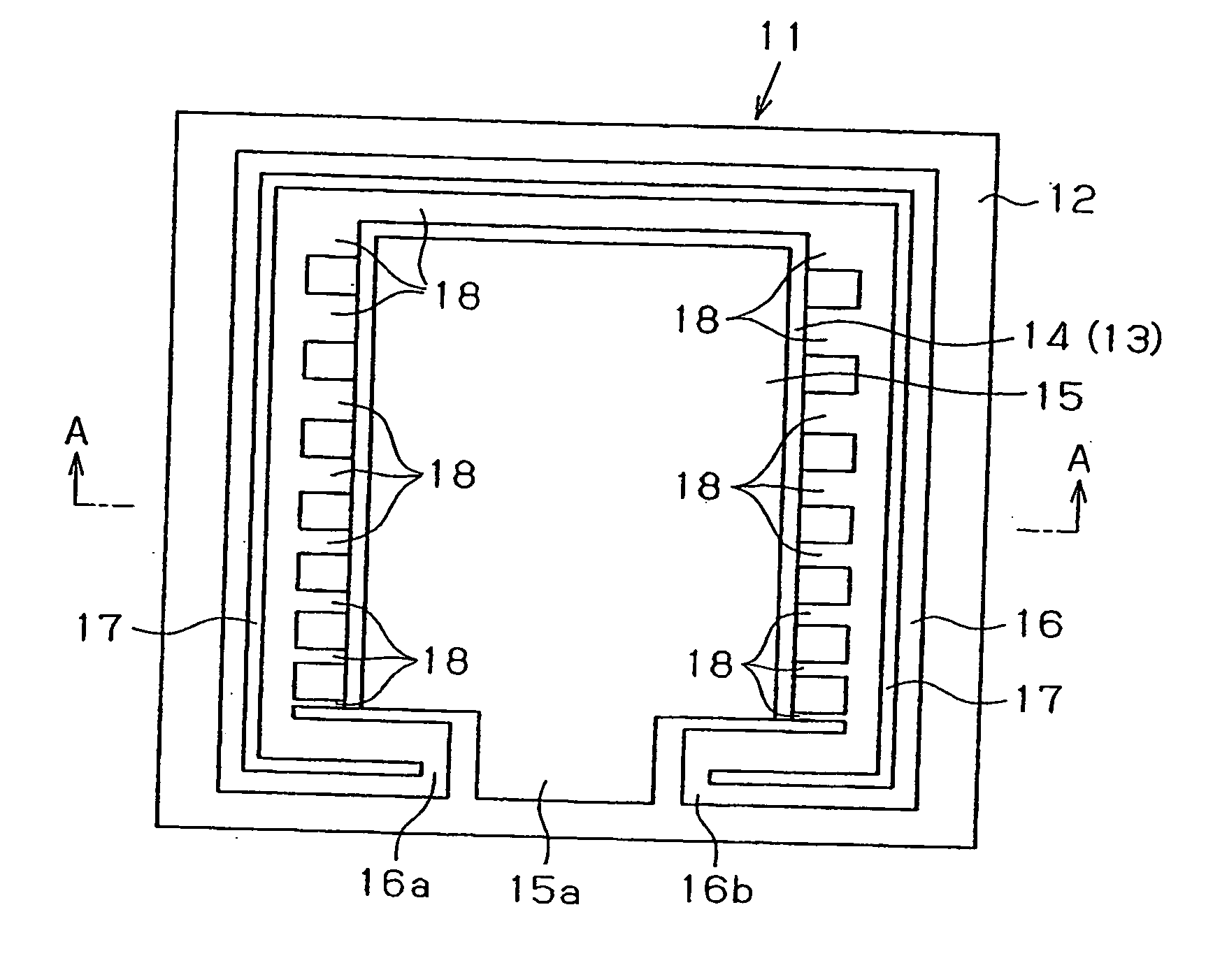
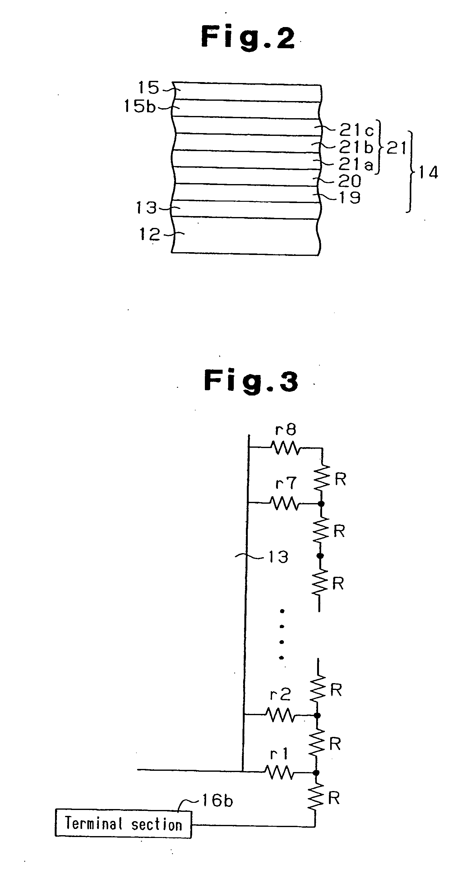
[0036] Each of the first electrode 13, the organic light emission layer 14, and the second electrode 15 has a substantially rectangular shape. The organic light emission layer 14 and the first electrode 13 have substantially equal surface areas. The second electrode 15 has a smaller surface area than that of the organic light emission layer 14 for preventing a short circuit between the second electrode 15 and the first electrode 13. In the first embodiment, the first electrode 13 corresponds to an anode and the second electrode 15 corresponds to a cathode. The second electrode 15 has a terminal portion 15a formed in one side of the second electrode 15. The terminal portion 15a connects the second electrode 15 to an external driver circuit (non-illustrated).

[0037] The feeder portion 16 is formed on the substrate 12, extending along the outer circumference of the first electrode 13. The width of the feeder portion 16 is uniform. Two terminal portions 16a, 16b are formed at opposing en...

second embodiment

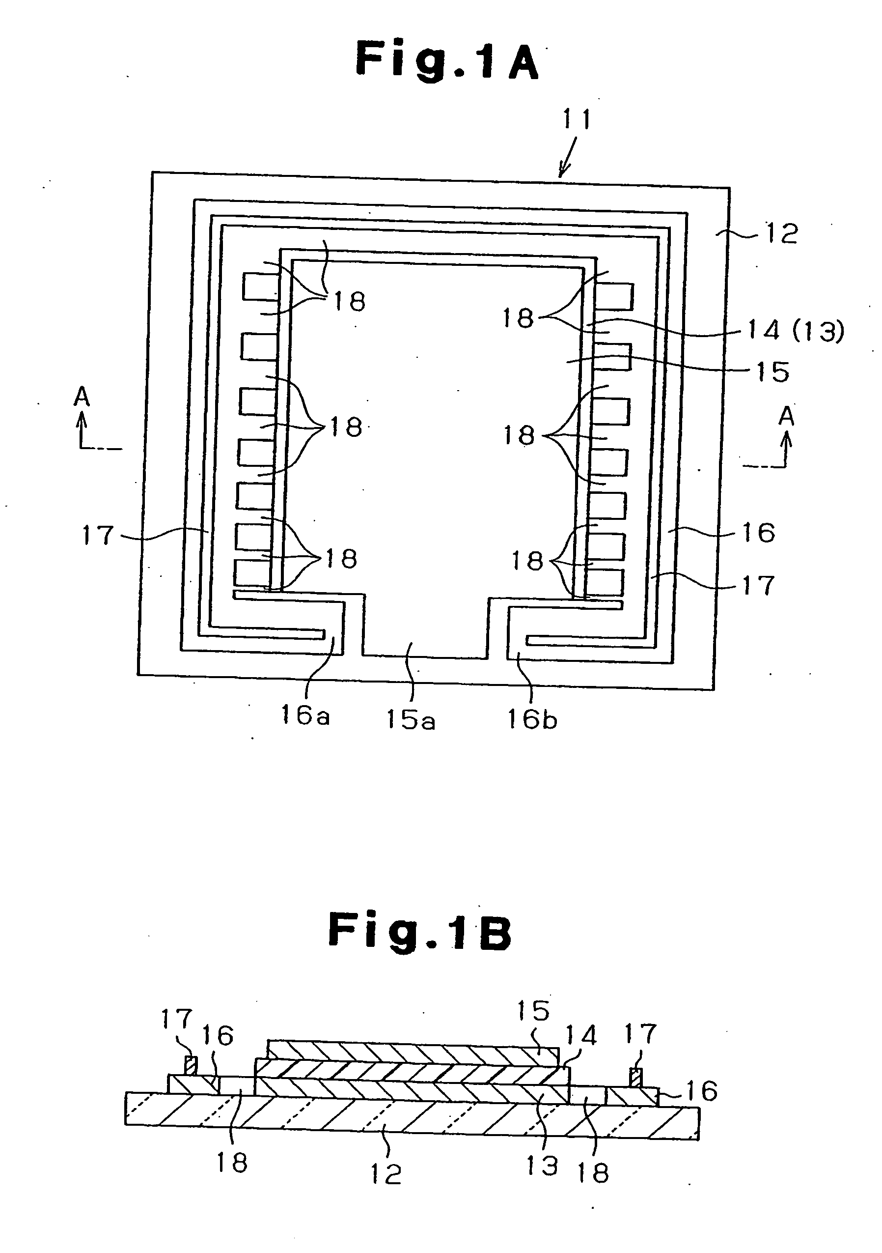
[0067]FIG. 4 is a plan view showing an organic EL element 22 of the second embodiment from which the organic light emission layer 14 and the second electrode 15 are removed. FIG. 5 is a cross-sectional view showing the structure of the non-light-emission portion of the organic EL element 22, by way of example.

[0068] As shown in FIG. 4, the organic EL element 22 includes a plurality of non-light-emission portions 23. The distribution density of the non-light-emission portions 23 becomes smaller from the outer circumferential portion of the first electrode 13 towards the center. Referring to FIG. 5, the non-light-emission portions 23 are defined by not providing the first electrode 13 at the corresponding portions in the second embodiment. Further, it is preferable that the size of each of the non-light-emission portions 23 be sufficiently small so that the non-light-emission portions 23 are invisible from the exterior of the organic EL element 22.

[0069] The non-light-emission portio...

third embodiment

[0076] As shown in FIGS. 6A and 6B, the organic EL element 24 has a single connector portion 18 that connects the feeder portion 16 to the first electrode 13. The thicknesses of portions of the connector portion 18 corresponding to opposing left and right sides of the first electrode 13 vary continuously. For example, in the third embodiment, the thickness of each of these portions of the connector portion 18 becomes greater as the position farther from the corresponding terminal portion 16a, 16b. Such thickness becomes gradually smaller towards the terminal portion 16a, 16b. Thus, a resistance value per unit length of the connector portion 18 as measured along a direction in which the feeder portion 16 extends becomes lower as the position farther from the terminal portion 16a, 16b. Such value becomes higher as the position closer to the terminal portion 16a, 16b. In other words, the feeder portion 16 extends along one side of the first electrode 13. The resistance value of the con...


PUM


Abstract

An electroluminescence element includes a first electrode, a second electrode, and a light emission layer arranged between the first electrode and the second electrode. The first electrode is formed of a material having a higher volume resistivity than that of the material of the second electrode. A connector portion electrically connects a feeder portion to the first electrode. The resistance value of the connector portion differs in correspondence with a position at which the connector portion connects the feeder portion to the first electrode. The brightness distribution of the electroluminescence element is thus adjusted to a desired state.

Description

BACKGROUND OF THE INVENTION [0001] The present invention relates to electroluminescence elements. [0002] Organic electroluminescence elements (hereinafter, referred to as “organic EL elements”) are employed in displays and lighting devices as light emission elements. One such element basically includes an anode electrode layer, an organic light emission layer, and a cathode electrode layer, which are deposited on a transparent substrate formed of, for example, glass in this order. [0003] The organic EL element emits light when voltage is applied between the anode electrode layer and the cathode electrode layer and thus an electric current flows in the organic light emission layer. Typically, the light emitted by the organic light emission layer passes through an electrode of the anode or cathode electrode layer and is thus sent to the exterior. In this case, at least the electrode through which the light passes is formed by a transparent electrode that transmits the light. The trans...

Claims


Application Information

Patent Timeline
Patent Type & Authority Applications(United States)
IPC IPC(8): H01L29/08
CPCH01L51/5203H01L2251/5361H01L27/3279H01L27/329H10K59/1315H10K59/1795H10K50/805H05B33/26
Inventor KAWAUCHI, HIROYASUHARADA, MASAYUKITAKEUCHI, NORIHITOHIEDA, MASATO
Owner TOYOTA IND CORP
Why Eureka
Try Eureka