In situ growth of oxide and silicon layers

a silicon layer and oxide technology, applied in the direction of polycrystalline material growth, crystal growth process, after-treatment details, etc., can solve the problems of reducing the tolerance for imperfections in semiconductor processing, affecting the crystal structure of the epitaxial layer, and affecting the growth of the polycrystalline material

Inactive Publication Date: 2005-09-22
ASM IP HLDG BV
View PDF58 Cites 8 Cited by
  • Summary
  • Abstract
  • Description
  • Claims
  • Application Information

AI Technical Summary

Benefits of technology

[0010] These and other needs are satisfied

Problems solved by technology

Recent advances in miniaturization and attendant circuit density, however, have lowered tolerances for imperfections in semiconductor processing.
Contaminants at the substrate surface can interfere with the crystal structure of the epita

Method used


Image

  • In situ growth of oxide and silicon layers
  • In situ growth of oxide and silicon layers
  • In situ growth of oxide and silicon layers

Examples


Embodiment Construction

[0023] While the preferred embodiments are discussed in the context of single-substrate, epitaxial silicon deposition, it will be understood that certain aspects of the invention will have application to non-epitaxial layers and deposition reactors of other types. Furthermore, while a series of process steps are disclosed herein for treating a single substrate, one of ordinary skill in the art will recognize the utility of certain of the disclosed steps even in the absence of some of the disclosed steps.

Preferred Reactor

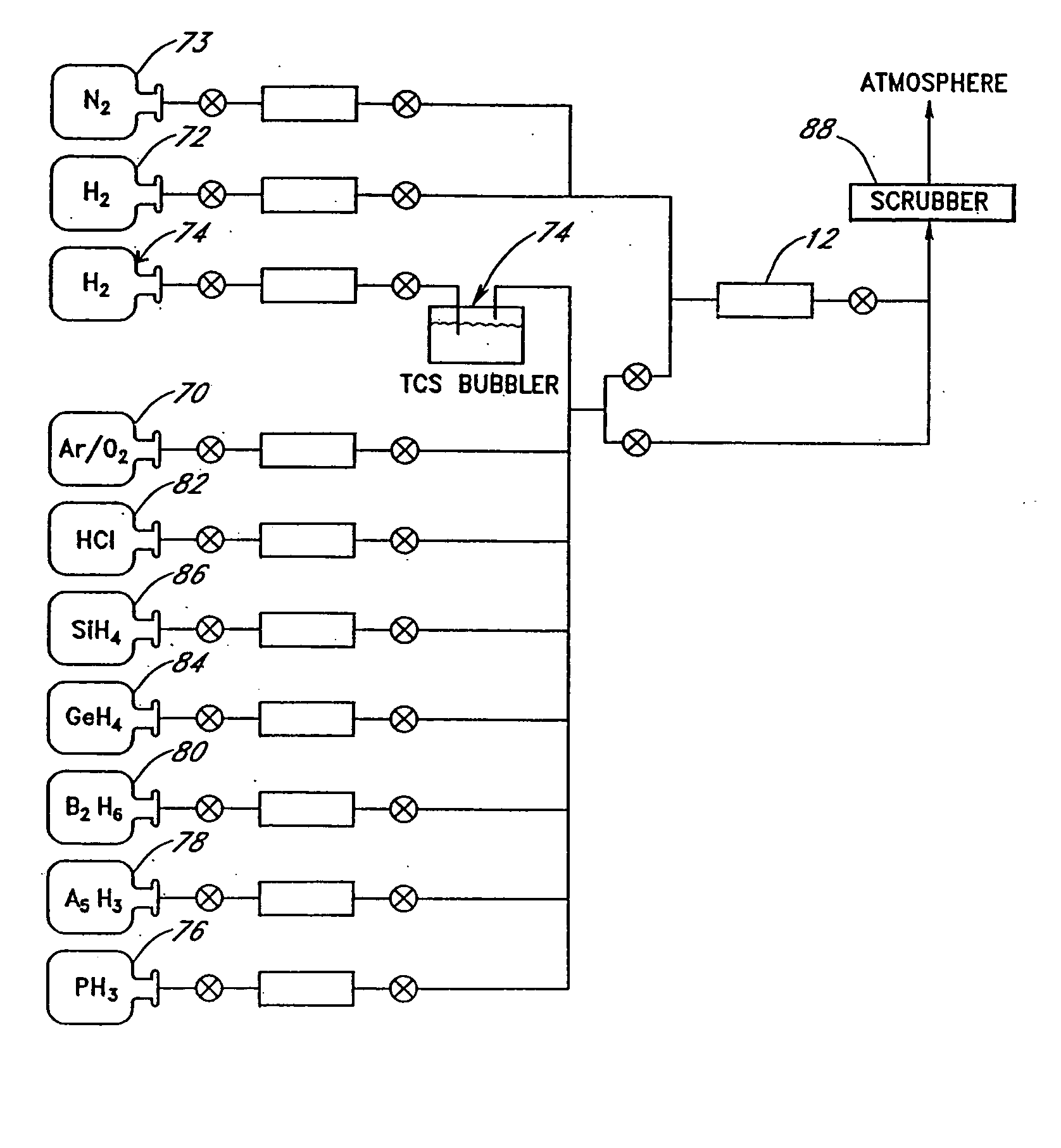
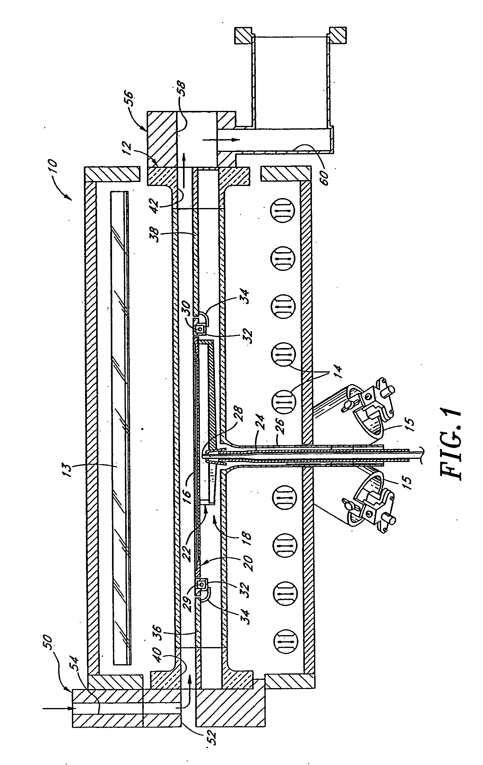
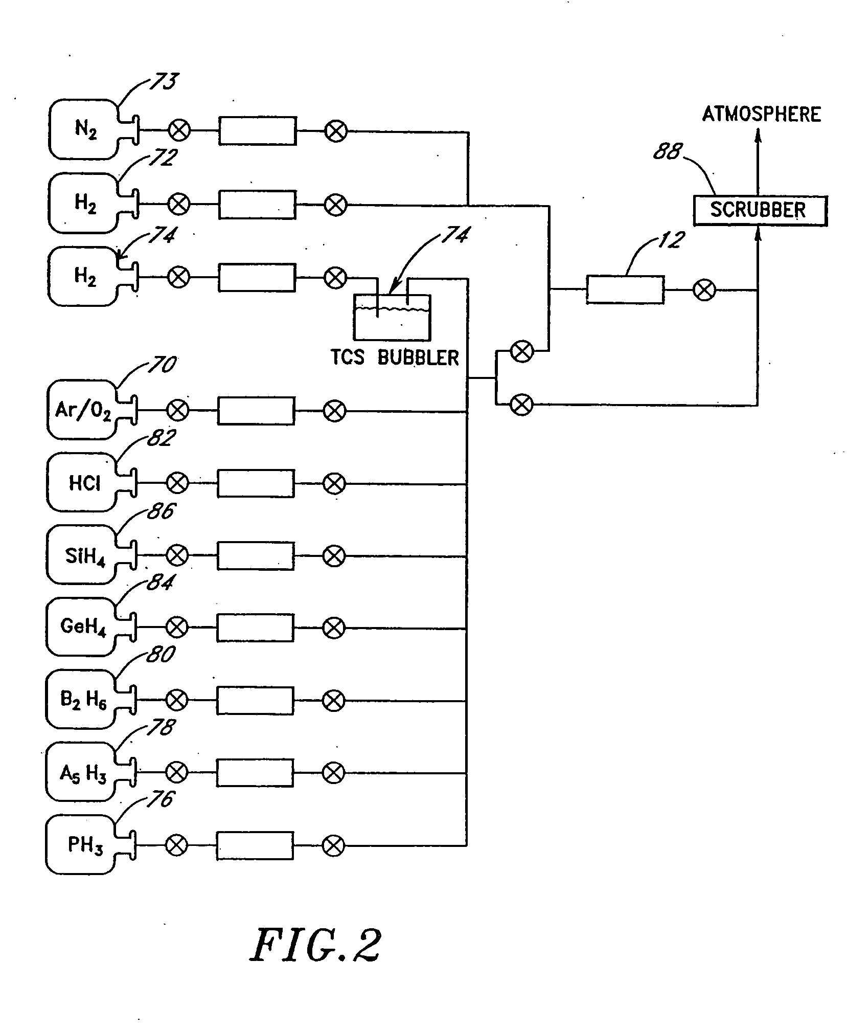
[0024]FIG. 1 shows a chemical vapor deposition (CVD) reactor 10, including a quartz process or reaction chamber 12, constructed in accordance with a preferred embodiment, and for which the methods disclosed herein have particular utility. The illustrated reactor 10 is specifically designed to optimize epitaxial deposition of silicon on a single substrate at a time, though it can also be employed for CVD of a number of different types of layers, as will be apparent...


PUM

PropertyMeasurementUnit
Lengthaaaaaaaaaa
Fractionaaaaaaaaaa
Diameteraaaaaaaaaa

Abstract

A single-wafer, chemical vapor deposition reactor is provided with hydrogen and silicon source gas suitable for epitaxial silicon deposition, as well as a safe mixture of oxygen in a non-reactive gas. Methods are provided for forming oxide and silicon layers within the same chamber. In particular, a sacrificial oxidation is performed, followed by a hydrogen bake to sublime the oxide and leave a clean substrate. Epitaxial deposition can follow in situ. A protective oxide can also be formed over the epitaxial layer within the same chamber, preventing contamination of the critical epitaxial layer. Alternatively, the oxide layer can serve as the gate dielectric, and a polysilicon gate layer can be formed in situ over the oxide.

Description

REFERENCE TO RELATED APPLICATION [0001] This application is a continuation of U.S. patent application Ser. No. 10 / 293,795, filed Nov. 12, 2002, which is a continuation of application Ser. No. 09 / 227,679, filed Jan. 8, 1999 (now U.S. Pat. No. 6,749,687), which claims the priority benefit of U.S. Provisional Application No. 60 / 070,991, filed Jan. 9, 1998.FIELD OF THE INVENTION [0002] The present invention relates to forming oxide and silicon layers within a single semiconductor processing chamber, and more particularly to thermal oxidation within a single-wafer epitaxial silicon deposition chamber. BACKGROUND OF THE INVENTION [0003] High-temperature ovens, called reactors, are used to create structures of very fine dimensions, such as integrated circuits on semiconductor substrates. One or more substrates, such as silicon wafers, are placed on a wafer support inside the reaction chamber. Both the wafer and support are heated to a desired temperature. In a typical wafer treatment step,...

Claims


Application Information

Patent Timeline
IPC IPC(8): C23C16/00C23C16/44C23C16/48C30B25/02C30B25/14C30B29/06H01L21/205H01L21/28H01L21/311H01L21/316H01L21/336
CPCC23C16/4405H01L21/02661C30B25/02C30B25/14C30B29/06H01L21/02238H01L21/02255H01L21/02301H01L21/02332H01L21/02337H01L21/28017H01L21/31116H01L21/31612H01L21/31662H01L29/66651H01L21/02381H01L21/02532H01L21/0262C23C16/481H01L21/02576H01L21/02579C30B25/105C30B33/005C30B33/02C30B33/12
Inventor FERRO, ARMANDRAAIJMAKERS, IVOFOSTER, DERRICK
Owner ASM IP HLDG BV
Why Eureka
Try Eureka