
Chemical agent additives in copper CMP slurry

a technology of additives and chemical agents, applied in the direction of electrical equipment, decorative surfaces, decorative arts, etc., can solve the problems of non-uniform surface of planarized copper, difficult to work with cu, and use of cmp methods versus reactive ion etching, so as to reduce dishing and non-uniform surface

Inactive Publication Date: 2005-09-22
CHARTERED SEMICONDUCTOR MANUFACTURING
View PDF14 Cites 8 Cited by
  • Summary
  • Abstract
  • Description
  • Claims
  • Application Information

AI Technical Summary

Benefits of technology

[0011] Accordingly, it is an object of the present invention to provide a Cu CMP slurry that reduces dishing and non-uniform surfaces.

Problems solved by technology

As copper (Cu) begins to replace aluminum (Al) as a wiring material due to copper's lower resistivity, the difficulty of working with Cu requires the use of CMP methods versus reactive-ion etching.
However, Cu is so soft that the polishing rate is still fast, causing dishing and non-uniform surfaces of the planarized copper.

Method used


Image

  • Chemical agent additives in copper CMP slurry
  • Chemical agent additives in copper CMP slurry
  • Chemical agent additives in copper CMP slurry

Examples


Embodiment Construction

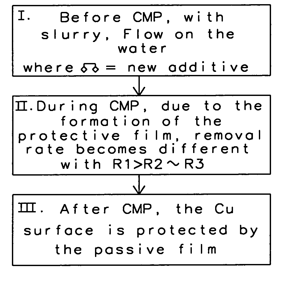
[0023] It is important when forming via holes, contact holes, or buried metal wiring portions by polishing a substrate that has protruding and recessed portions that only the protruding portions are polished so as to leave a desired film only in the recessed portions. If only mechanical polishing is used then the desired effect of having the film remaining only in the recessed portions is efficiently achieved ensuring a high selective ratio. However, the throughput necessary in a semiconductor device manufacturing step cannot be ensured due to the low polishing rate of mechanical polishing. If only chemical polishing is used instead of mechanical polishing then the film fails to remain only in the recessed portions and the desired effect is not achieved despite a high polishing rate since etching proceeds isotropically, i.e. the etching process attacks the layer surface equally in all directions.

[0024] Thus a combination of mechanical and chemical polishing, i.e. chemical mechanica...


PUM

PropertyMeasurementUnit
weight %aaaaaaaaaa
weight %aaaaaaaaaa
conductiveaaaaaaaaaa

Abstract

A polishing method is achieved comprising the following steps. A layer made of material containing a metal as a main component over a substrate having recessed portions on a surface thereof so as to fill the recessed portions with the metal layer is formed. The metal is Cu, a Cu alloy, Al, or an Al alloy. The metal layer is polished by a chemical mechanical polishing method using a slurry including a polishing agent. The polishing agent contains a chemical agent and an etching agent. The chemical agent includes at least a carbonyl derivative of benzotriazole and is responsible for forming a protective film on the surface of the metal layer by reacting with the material containing a metal as a main component. The etching agent is responsible for etching the material containing a metal as a main component.

Description

FIELD OF THE INVENTION [0001] The present invention relates generally to a chemical mechanical polishing (CMP) polishing method, and more specifically to a polishing method using a polishing agent for use in CMP of a semiconductor device in a micro-processing step. BACKGROUND OF THE INVENTION [0002] Chemical mechanical polishing (CMP) is used to planarize various levels of multi-layered semiconductor devices to permit the smaller designs used to fabricate ever miniaturized semiconductor devices. For example, CMP is used to form planar interlayer insulating films, buried wiring portions and metal plugs. As copper (Cu) begins to replace aluminum (Al) as a wiring material due to copper's lower resistivity, the difficulty of working with Cu requires the use of CMP methods versus reactive-ion etching. [0003] Recently, benzotriazole (C6H5N3) (BTA) (See FIG. 1A) has been used for copper CMP due to benzotriazole's ability to form a protective polymeric layer of Cu (I) BTA. This helps to red...

Claims


Application Information

Patent Timeline
Patent Type & Authority Applications(United States)
IPC IPC(8): B44C1/22C09G1/02C23F1/00C23F3/06
CPCC23F3/06C09G1/02
Inventor HO, PAUL KWOK KEUNGZHOU, MEI SHENGRAMASAMY, CHOCKALINGAM
Owner CHARTERED SEMICONDUCTOR MANUFACTURING
Learn More