Flip chip bonded micro-electromechanical system (MEMS) device

a micro-electromechanical system and chip bonded technology, applied in the direction of fluid speed measurement, acceleration measurement using interia forces, instruments, etc., can solve the problems of mechanical damage, stiction problems in the finished device, and sensitiveness of the mems devi

Inactive Publication Date: 2005-09-22
HONEYWELL INT INC
View PDF16 Cites 118 Cited by
  • Summary
  • Abstract
  • Description
  • Claims
  • Application Information

AI Technical Summary

Benefits of technology

[0031] According to another aspect of the invention, the semiconductor silicon mechanism substrate having the micro-machined capacitive acceleration sensor mechanism patterned therein is mechanically coupled to the inner surface of the top substrate; the one or more mesas extend from the inner surface of the top substrate; and the plurality of wire bond pads are formed on the inner surface of the bottom substrate in an area remote from the sensor mechanism.

Problems solved by technology

Moving parts within a device are typically separated by microscopically narrow critical gap spacings, and as such are highly sensitive to particle contamination, such as dust and other microscopic debris.
MEMS devices are also sensitive to contamination arising from corrosive environments; humidity and H2O in either the liquid or vapor phase, which may cause stiction problems in the finished device; and mechanical damage such as abrasion.
Each of the individual processes may expose the device to a source of contamination.
This sensitivity to particle contamination poses a challenge to the structural design and microfabrication processes associated with these small-scale, intricate and precise devices in view of the desire to have fabrication repeatability, fast throughput times, and high product yields from high-volume manufacturing.
These internal windows may allow particulate contamination or moisture to invade the interior of the MEMS device during handling, transportation, testing or wire bonding operations, which can result in premature failure.
These internal apertures 36 can allow particulate contamination or moisture to invade the interior of the MEMS device 10 during handling, transportation, testing or wire bonding operations, which can result in premature failure.
These signal routing limitations demand very complex designs to accommodate communication with the upper device mechanism and substrate surfaces 28, 32.
In some MEMS devices these signal routing limitations limit their performance as sensors.
For example, the inability to communicate with one side of the device causes it to have asymmetric response which tends to degrade performance, particularly in a vibration environment.
Additionally, the inability to provide the restoring forces of electrostatic attraction between the top surface 28 of the device mechanism 16 and the top cover plate 20 because of the communication limitations increases the complexity of closed-loop sensor designs.

Method used


Image

  • Flip chip bonded micro-electromechanical system (MEMS) device
  • Flip chip bonded micro-electromechanical system (MEMS) device
  • Flip chip bonded micro-electromechanical system (MEMS) device

Examples


Embodiment Construction

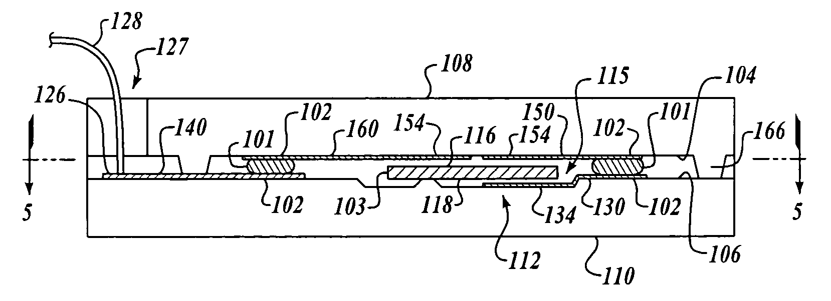
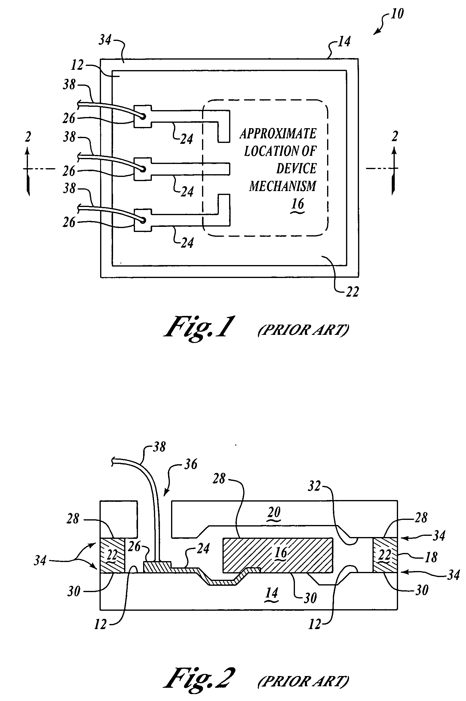
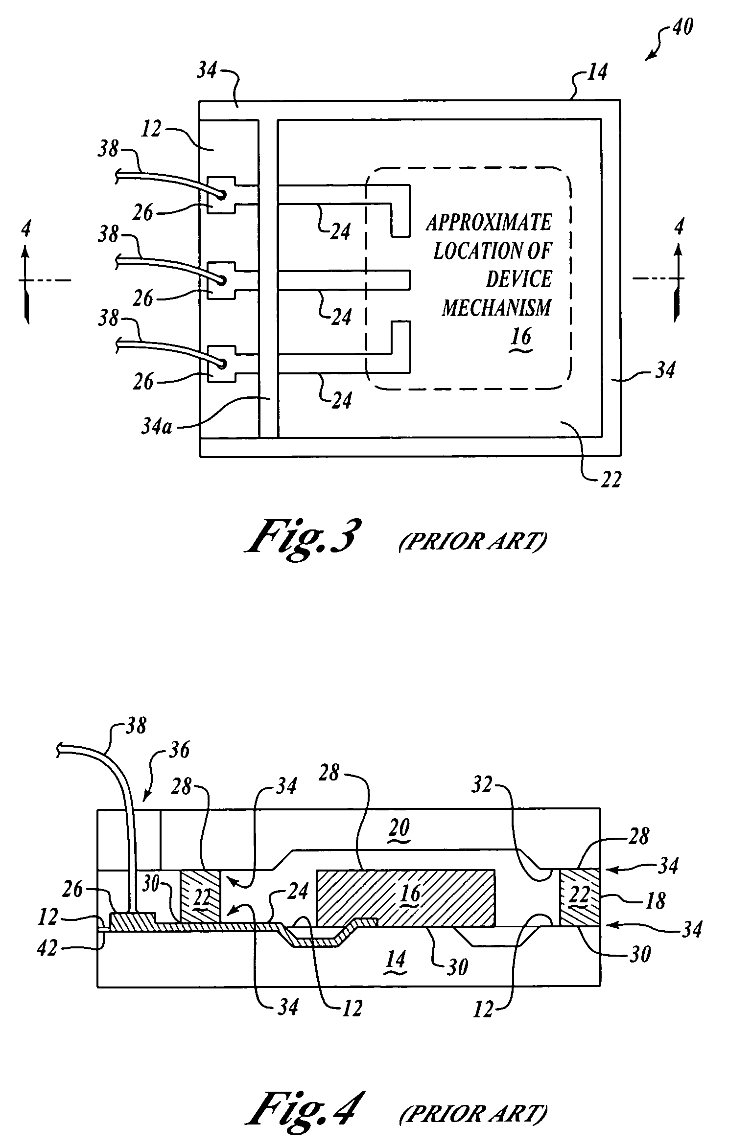
[0042] In the Figures, like numerals indicate like elements.

[0043] The present invention is an apparatus and method for communicating between opposing top and bottom surfaces of micro-electromechanical system (MEMS) devices by means of a plurality of conductive stud bumps on chip bond pads.

[0044] The use of conductive stud bumps on chip bond pads is well-known in the electronics industry for making electrical connections in microelectronic assemblies. Flip chip microelectronic assembly is the formation of direct electrical connection of face-down electronic components onto substrates, circuit boards, or carriers, by means of conductive bumps on chip bond pads. The flip chip technology, also known as Direct Chip Attach (DCA), replaces older wire bonding technology in semiconductor device assemblies which uses face-up chips with wire connections to the bond pads. Furthermore, wire bond connections are limited to the perimeter of the die, while flip chip connections can be made anywh...


PUM


Abstract

A micro-electromechanical system (MEMS) device having a pair of spaced apart top and bottom substrates or cover plates having mutually opposing inner surfaces structured to cooperate with a micro-machined electromechanical device mechanism, such as a micro-machined sensor or actuator mechanism. Such a micro-machined electromechanical device mechanism is coupled to the inner surface of one of the top and bottom substrates. A metal chip bond pad is formed on the inner surface of the bottom substrate and is electrically coupled to an electrical path; another metal chip bond pad formed on the inner surface of the top substrate in a complementary position opposite the chip bond pad on the bottom substrate; and an electrically conductive gold stud bump is mechanically and electrically coupled between the metal chip bond pads on the top and bottom substrates.

Description

FIELD OF THE INVENTION [0001] The present invention relates generally to devices fabricated as micro-electromechanical system (MEMS) devices and methods for manufacturing the same, and in particular to double-sided MEMS devices and methods for both mechanically attaching operational protective covers to MEMS devices and routing signals therethrough. BACKGROUND OF THE INVENTION [0002] Many devices fabricated as micro-electromechanical systems (MEMS), both sensor and actuator devices, and methods for manufacturing the same are generally well-known. See, for example, U.S. patent application Ser. No. 09 / 963,142, METHOD OF TRIMMING MICRO-MACHINED ELECTROMECHANICAL SENSORS (MEMS) DEVICES, filed in the name of Paul W. Dwyer on Sep. 24, 2001, which is assigned to the assignee of the present application and the complete disclosure of which is incorporated herein by reference, that describes a MEMS acceleration sensor and method for manufacturing the same. In another example, U.S. Pat. No. 6,...

Claims


Application Information

Patent Timeline
Patent Type & Authority Applications(United States)
IPC IPC(8): B81B7/00H01L23/10H01L29/84
CPCB81B7/007B81B2207/097H01L24/45H01L2224/45144H01L2224/48091H01L2924/01014H01L2924/01322H01L2924/3025H01L2924/01079H01L2924/07802H01L2924/10253H01L2924/01013H01L2924/00014H01L2924/00H01L2224/45015
Inventor ESKRIDGE, MARK H.
Owner HONEYWELL INT INC
Why Eureka
Try Eureka