Method of forming a capacitor

a capacitor and insulating layer technology, applied in the field of chemical and physical vapor deposition methods, can solve the problems of increasing current leakage, hurting leakage characteristics, and unsuitable dielectrics such as siosub>2/sub>nsub>4/sub>nsub>4/sub>

Inactive Publication Date: 2005-09-22
MICRON TECH INC
View PDF83 Cites 301 Cited by
  • Summary
  • Abstract
  • Description
  • Claims
  • Application Information

AI Technical Summary

Problems solved by technology

As DRAMs increase in memory cell density, there is a continuing challenge to maintain sufficiently high storage capacitance despite decreasing cell area.
The feature size of 256 Mb DRAMs and beyond will be on the order of 0.25 micron or less, and conventional dielectrics such as SiO2 and Si3N4 might not be suitable because of small dielectric constants.
In some materials, aspects of a high k material which might be modified or tailored to achieve a highest capacitor dielectric constant possible will unfortunately also tend to hurt the leakage characteristics (i.e., increase current leakage).
Accordingly, capacitance can be increased by increasing the concentration of barium and / or strontium, but unfortunately at the expense of increasing leakage.
Further, absence of titanium in the oxide lattice creates a metal vacancy in such multimetal titanates which can increase the dielectric constant, but unfortunately also increases the current leakage.

Method used


Image

  • Method of forming a capacitor
  • Method of forming a capacitor
  • Method of forming a capacitor

Examples


Embodiment Construction

[0017] This disclosure of the invention is submitted in furtherance of the constitutional purposes of the U.S. Patent Laws “to promote the progress of science and useful arts” (Article 1, Section 8).

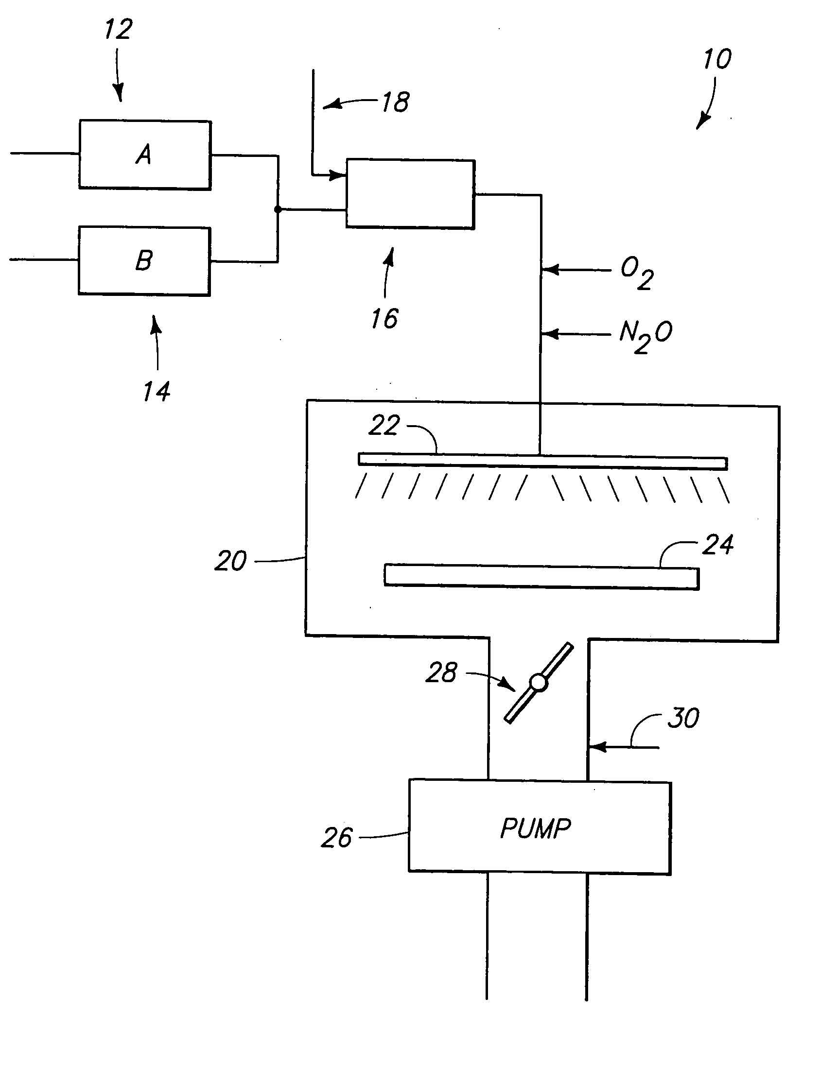
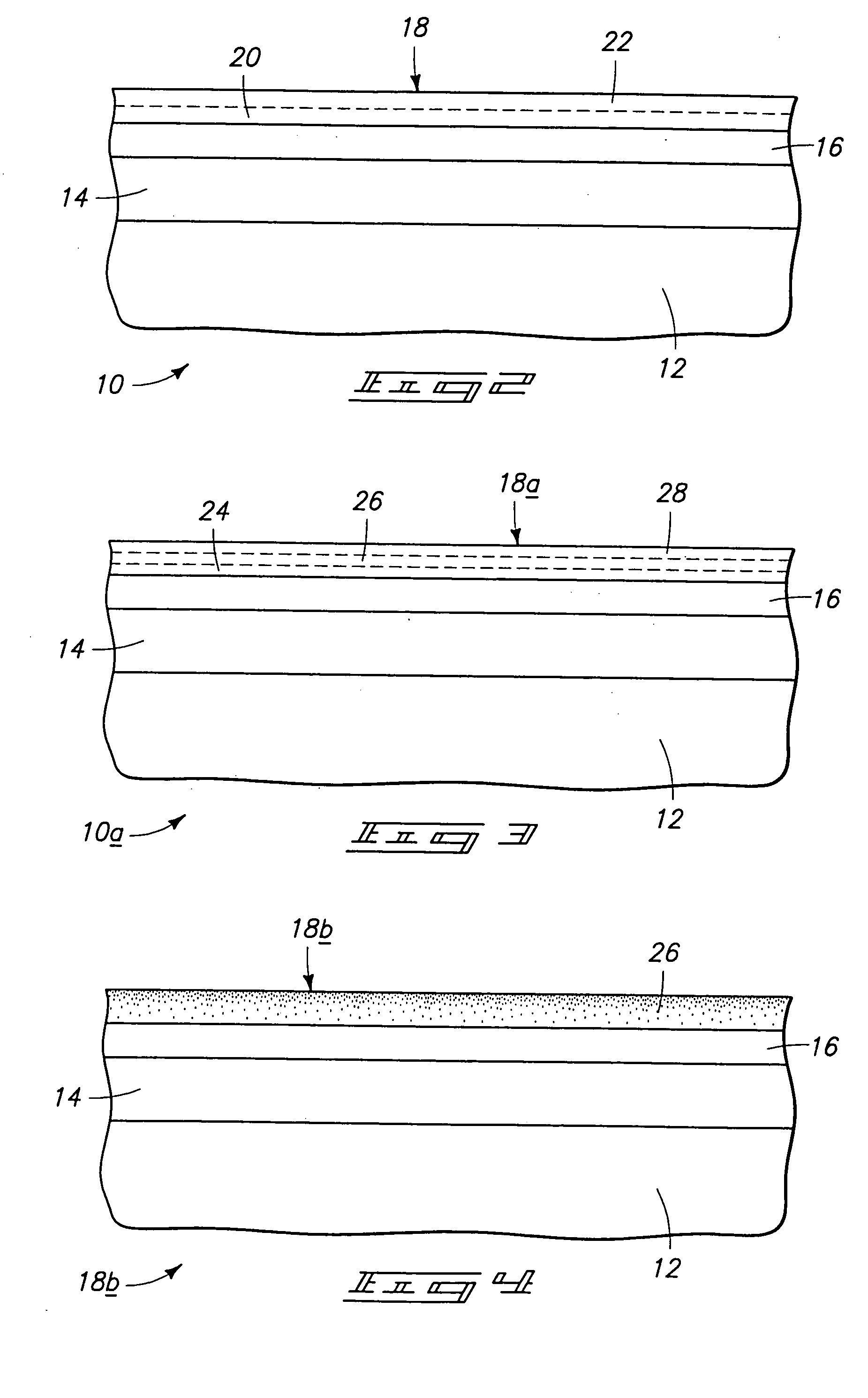
[0018] The prior art recognizes the desirability in certain instances of fabricating high k dielectric regions of capacitors, such as ABO3 layers as referred to above, to have variable concentration at different elevational locations in the thickness of such regions of the “A” and “B” components. For example with respect to titanates, the quantity of titanium represented by the variable “B” in ABO3 is impacting relative to leakage current characteristics and k value in the subject layer. Accordingly in some instances, it might be desirable to fabricate a capacitor dielectric region to have one elevational range of one ABO3 stoichiometry, and another elevational range of the region to have a different ABO3 stoichiometry, utilizing the same or different combinations of elements. Further, ...


PUM

PropertyMeasurementUnit
sizeaaaaaaaaaa
pressureaaaaaaaaaa
pressureaaaaaaaaaa

Abstract

The invention includes chemical vapor deposition and physical vapor deposition methods of forming high k ABO3 comprising dielectric layers on a substrate, where “A” is selected from the group consisting of Group IIA and Group IVB elements and mixtures thereof, and where “B” is selected from the group consisting of Group IVA metal elements and mixtures thereof. In one implementation, a plurality of precursors comprising A, B and O are fed to a chemical vapor deposition chamber having a substrate positioned therein under conditions effective to deposit a high k ABO3 comprising dielectric layer over the substrate. During the feeding, pressure within the chamber is varied effective to produce different concentrations of A at different elevations in the deposited layer and where higher comparative pressure produces greater concentration of B in the deposited layer. In one implementation, a subatmospheric physical vapor deposition method of forming a high k ABO3 comprising dielectric layer on a substrate includes providing a sputtering target comprising ABO3 and a substrate to be deposited upon within a physical vapor deposition chamber. A sputtering gas is fed to the chamber under conditions effective to sputter the target and deposit a high k ABO3 comprising dielectric layer over the substrate. During the feeding, pressure is varied within the chamber effective to produce different concentrations of B at different elevations in the deposited layer and where higher comparative pressure produces greater concentration of B in the deposited layer.

Description

TECHNICAL FIELD [0001] This invention relates to chemical and physical vapor deposition methods of forming high k ABO3 comprising dielectric layers on a substrate, where “A” is selected from the group consisting of Group IIA and Group IVB elements and mixtures thereof, and where “B” is selected from the group consisting of Group IVA metal elements and mixtures thereof. BACKGROUND OF THE INVENTION [0002] As DRAMs increase in memory cell density, there is a continuing challenge to maintain sufficiently high storage capacitance despite decreasing cell area. Additionally, there is a continuing goal to further decrease cell area. One principal way of increasing cell capacitance is through cell structure techniques. Such techniques include three-dimensional cell capacitors, such as trenched or stacked capacitors. Yet as feature size continues to become smaller and smaller, development of improved materials for cell dielectrics as well as the cell structure are important. The feature size ...

Claims


Application Information

Patent Timeline
Patent Type & Authority Applications(United States)
IPC IPC(8): C23C14/08C23C16/00C23C16/40C23C16/44C23C16/455H01L21/02
CPCC23C14/088C23C14/3492H01L28/55C23C16/45523C23C16/45557C23C16/409
Inventor BASCERI, CEM
Owner MICRON TECH INC
Why Eureka
Try Eureka