

Photoelectric conversion film-stacked type solid-state imaging device, method for driving the same and digital camera
a technology of solid-state imaging and photoelectric conversion, which is applied in the direction of radio frequency controlled devices, television system scanning details, television systems, etc., can solve the problems of reducing light utilization efficiency, reducing sensitivity, and reducing the total area of the photo acceptance portion, so as to achieve high sensitivity image, high resolution image, and high resolution
- Summary
- Abstract
- Description
- Claims
- Application Information
AI Technical Summary
Benefits of technology
Problems solved by technology
Method used
Image

Examples
first embodiment
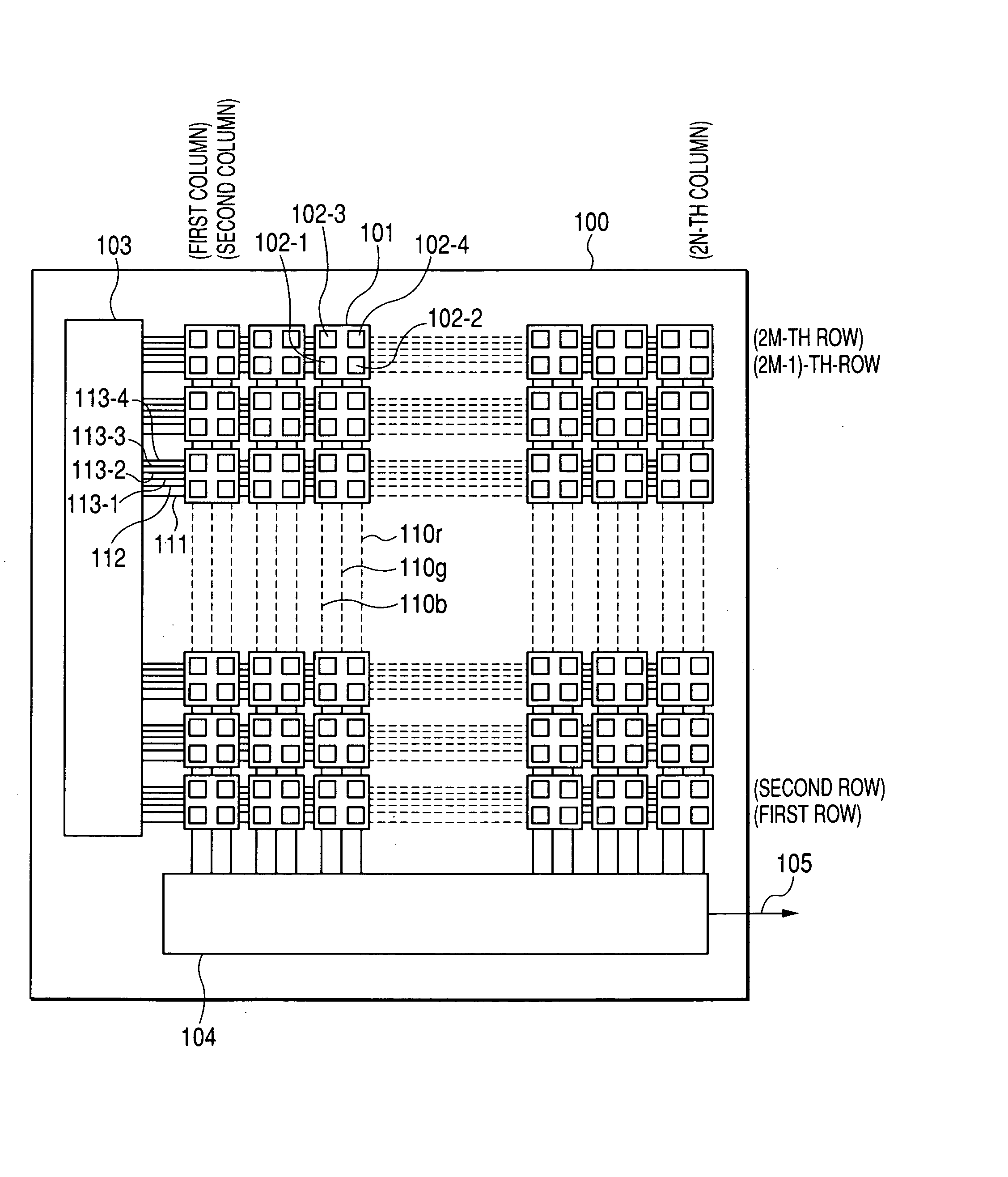
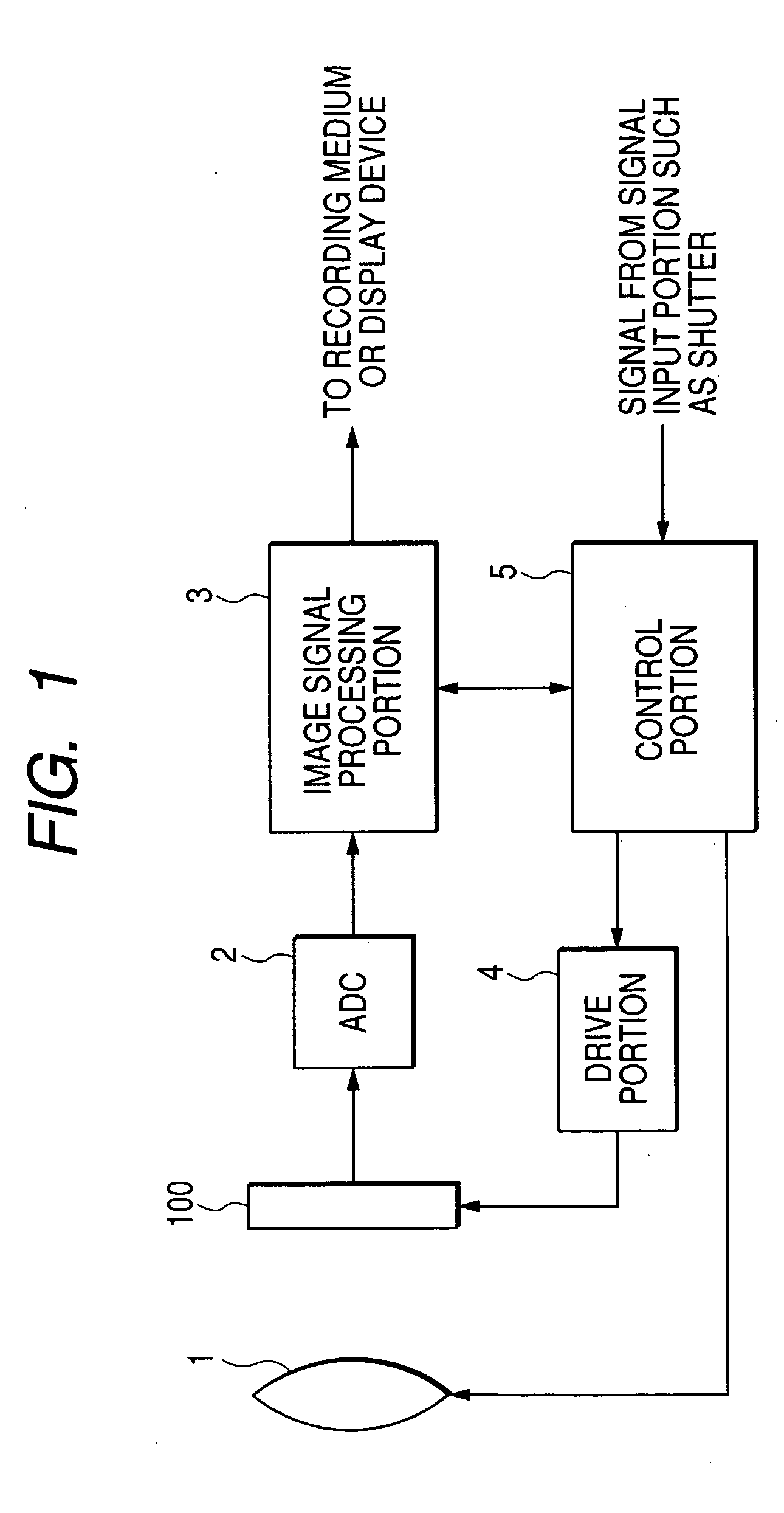
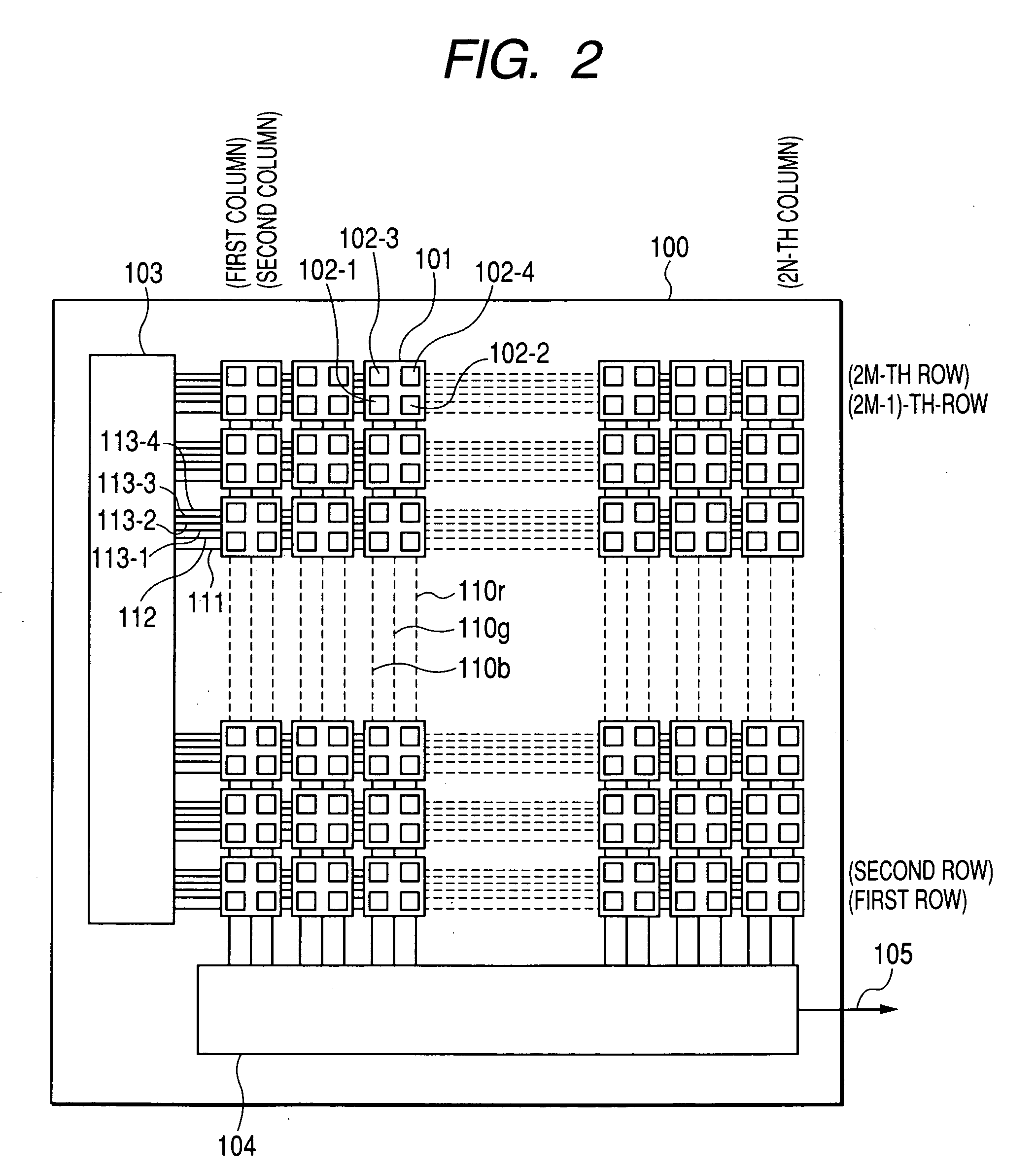
[0047]FIG. 1 is a block diagram of a digital camera in which a solid-state imaging device according to a first embodiment of the invention is mounted. The digital camera includes an image-forming optical system 1, a solid-state imaging device 100, an analog-to-digital converter 2, an image signal processing portion 3, a drive portion 4, and a control portion 5. The image-forming optical system 1 includes a photographic lens, an iris, and so on. The solid-state imaging device 100 will be described later in detail. The analog-to-digital converter 2 converts an analog image signal output from the solid-state imaging device 100 into a digital image signal. The image signal processing portion 3 performs image processing on the digital image signal and stores the processed image signal in a recording medium or displays the processed image signal on a display device. The drive portion 4 performs drive control on the solid-state imaging device 100. The control portion 5 takes in a signal fr...
second embodiment
[0088]FIG. 9 is a circuit configuration diagram of a signal readout circuit of a photoelectric conversion film lamination type solid-state imaging device according to a second embodiment. The configuration of the second embodiment is the same as that of the first embodiment except the configuration of each signal readout circuit.
[0089] In the first embodiment, the signal readout circuit as shown in FIG. 6 is configured so that red, green and blue signals are read out simultaneously while the signal readout circuit is divided into a red signal charge detection cell 109r, a green signal charge detection cell 109g and a blue signal charge detection cell 109b (i.e., a signal read out circuit corresponding to one unit 101 includes a plurality of output transistors). The second embodiment is different from the first embodiment in that a charge detection cell 109 is provided in common for respective colors and drains of twelve intra-unit pixel selection transistors 118-ir, 118-ig and 118-...
third embodiment
[0096]FIG. 10 is a circuit configuration diagram of a signal readout circuit according to a third embodiment of the invention. The configuration of the third embodiment is the same as that of the first or second embodiment except the configuration of the signal readout circuit.
[0097] The first or second embodiment may cause the following disadvantage. To capture a still image, a mechanical shutter has to be used. If an image signal is output after the mechanical shutter is closed after the image capturing, there is no problem. A problem will be, however, caused when the mechanical shutter cannot be used, for example, when a motion picture is captured.
[0098] In the state where signal charges in a certain color pixel become excessive because of a very bright subject, the excessive charges flow into a gate of an output transistor through a pixel selection transistor. Because the excessive charges are added to any other color signal, color mixture may occur to thereby result in deteri...
PUM
 Abstract
Description
Claims
Application Information