Liquid crystal display device

a liquid crystal display and display device technology, applied in the field of liquid crystal display devices, can solve the problems of parasitic capacitance increase, image sticking, and inability to use the passivation layer of the organic insulating layer for a small-sized lcd device such as a mobile phone, and achieve the effects of high optical density, high resolution, and preventing parasitic capacitan

Active Publication Date: 2005-10-06
LG DISPLAY CO LTD
View PDF19 Cites 49 Cited by
  • Summary
  • Abstract
  • Description
  • Claims
  • Application Information

AI Technical Summary

Benefits of technology

[0028] An advantage of the present invention is to provide an LCD device, to realize high resolution without light leakage by forming a first black matrix layer of a metal material having a high optical density and forming a second black matrix layer of resin to cover the first black matrix layer.
[0029] Additional advantages and features of the invention will be set forth in part in the description which follows and in part will become apparent to those having ordinary skill in the art upon examination of the following or may be learned from practice of the invention. The objectives and other advantages of the invention may be realized and attained by the structure particularly pointed out in the written description and claims hereof as well as the appended drawings.
[0030] To achieve these and other advantages and in accordance with the purpose of the invention, as embodied and broadly described herein, an LCD device includes a gate line on a first substrate; a gate insulating layer on an entire surface of the first substrate including the gate line; a data line on the gate insulating layer substantially perpendicular to the gate line, to define a pixel region; a thin film transistor at a crossing portion of the gate and data lines; a passivation layer on a surface of the first substrate including the thin film transistor; a pixel electrode on the passivation layer connected with a drain electrode of the thin film transistor; and a light-shielding metal preventing a parasitic capacitance between the data line and the pixel electrode.
[0032] In addition, the LCD device further includes a common line in parallel with the gate line. The light-shielding metal projects from the common line.
[0033] Also, the passivation layer is formed of an inorganic insulating material, wherein the inorganic insulating material is silicon nitride SiNx or silicon oxide SiOx.

Problems solved by technology

Thus, it is impossible to use the passivation layer of the organic insulating layer for a small-sized LCD device such as a mobile phone.
However, when using a passivation layer made of an inorganic insulating material, the parasitic capacitance increases greatly as compared with the passivation layer made of the organic insulating material, so that it is impossible to overlap the pixel electrode with the data line.
If the parasitic capacitance increases between the data line and the pixel electrode, the parasitic capacitance causes a D.C. voltage offset relative to an A.C. voltage applied to the liquid crystal layer, ΔVp, thereby generating flicker, image sticking, and non-uniformity of luminance in the images.
Because of the parasitic capacitance, a source delay is generated which decreases a data voltage level.
Thus, the luminance is changed due to the source delay, so that vertical crosstalk generates, thereby deteriorating the picture quality.

Method used


Image

  • Liquid crystal display device
  • Liquid crystal display device
  • Liquid crystal display device

Examples


Embodiment Construction

[0047] Reference will now be made in detail to embodiments of the present invention, examples of which are illustrated in the accompanying drawings. Wherever possible, the same reference numbers will be used throughout the drawings to refer to the same or like parts.

[0048] Hereinafter, an LCD device according to a first embodiment of the present invention will be described with reference to the accompanying drawings.

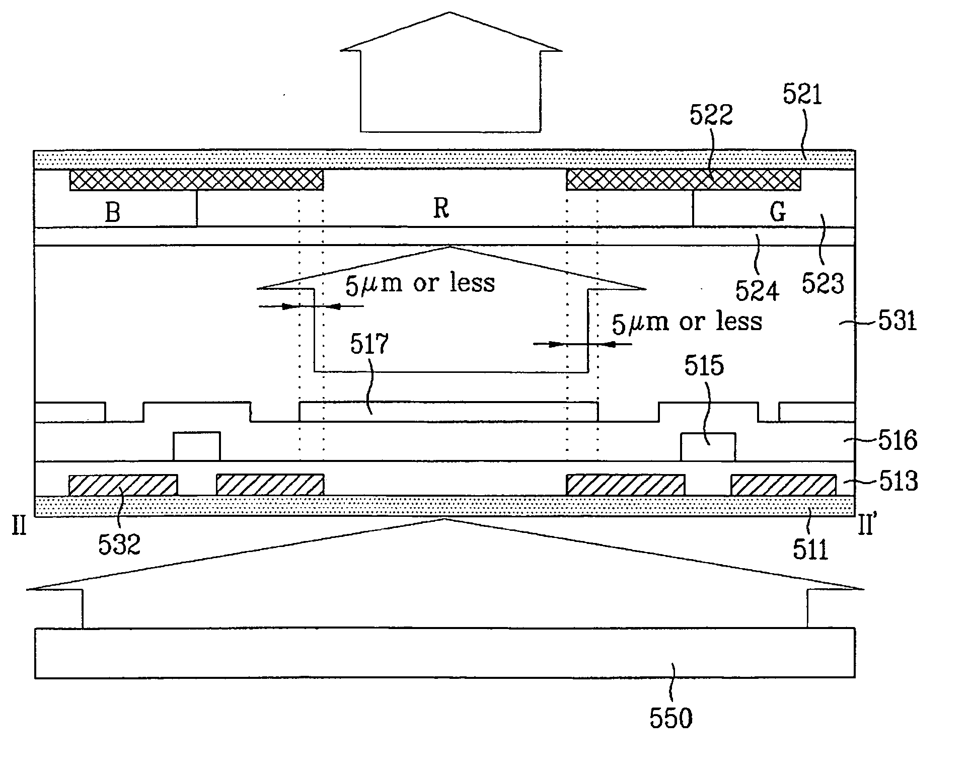
[0049]FIG. 3 is a plan view of an LCD device according to the first embodiment of the present invention. FIG. 4 is a cross sectional view of an LCD device along II-II′ of FIG. 3.

[0050] As illustrated in FIG. 3 and FIG. 4, the LCD device according to the first embodiment of the present invention includes a thin film transistor array substrate 511, a color filter array substrate 521, and a liquid crystal layer 531. The thin film transistor array substrate 511 and the color filter array substrate 521 are bonded to each other at a predetermined interval, and the liquid cr...


PUM

PropertyMeasurementUnit
thicknessaaaaaaaaaa
thicknessaaaaaaaaaa
dielectric constantaaaaaaaaaa

Abstract

An LCD device with improved an aperture ratio and decreased parasitic capacitance has a passivation layer of an inorganic material and which includes a gate line on a first substrate; a gate insulating layer on an entire surface of the first substrate including the gate line; a data line on the gate insulating layer in perpendicular to the gate line, to define a pixel region; a thin film transistor at a crossing portion of the gate and data lines; a passivation layer on the entire surface of the first substrate including the thin film transistor; a pixel electrode on the passivation layer, for being connected with a drain electrode of the thin film transistor; and a light-shielding metal for receiving a voltage, formed between the data line and the pixel electrode, to prevent a parasitic capacitance between the data line and the pixel electrode.

Description

[0001] This present invention claims the benefit of the Korean Application No. P2004-21678 filed on Mar. 30, 2004, which is hereby incorporated by reference for all purposes as if fully set forth herein. BACKGROUND OF THE INVENTION [0002] 1. Field of the Invention [0003] The present invention relates to a liquid crystal display (LCD) device, and more particularly, to an LCD device with improved aperture ratio and reduced parasitic capacitance. [0004] 2. Discussion of the Related Art [0005] LCD devices, one of a number of flat display technologies, have improved performance characteristics including high contrast ratio, great gray level, high picture quality, and low power consumption. [0006] For example, the LCD device having a thin profile may be fabricated in a wall-mountable type for a monitor of a television. Also, because the LCD device achieves light weight and low power consumption, the LCD device may be applicable as monitors for notebook computers, a personal computers, tel...

Claims


Application Information

Patent Timeline
Patent Type & Authority Applications(United States)
IPC IPC(8): G02F1/1368G02F1/136G02F1/1362
CPCG02F1/136209G02F2001/136218G02F1/136213G02F1/136218G02F1/133512B25H7/04
Inventor KWON, KEUK SANGPARK, DAE LIMHWANG, SEONG SOOKANG, SUNG GULEE, JONG HWAEKIM, BUNG GOOCHOI, JONG A.
Owner LG DISPLAY CO LTD
Why Eureka
Try Eureka