Marking system for a semiconductor wafer to identify problems in mask layers
- Summary
- Abstract
- Description
- Claims
- Application Information
AI Technical Summary
Problems solved by technology
Method used
Image

Examples
Embodiment Construction
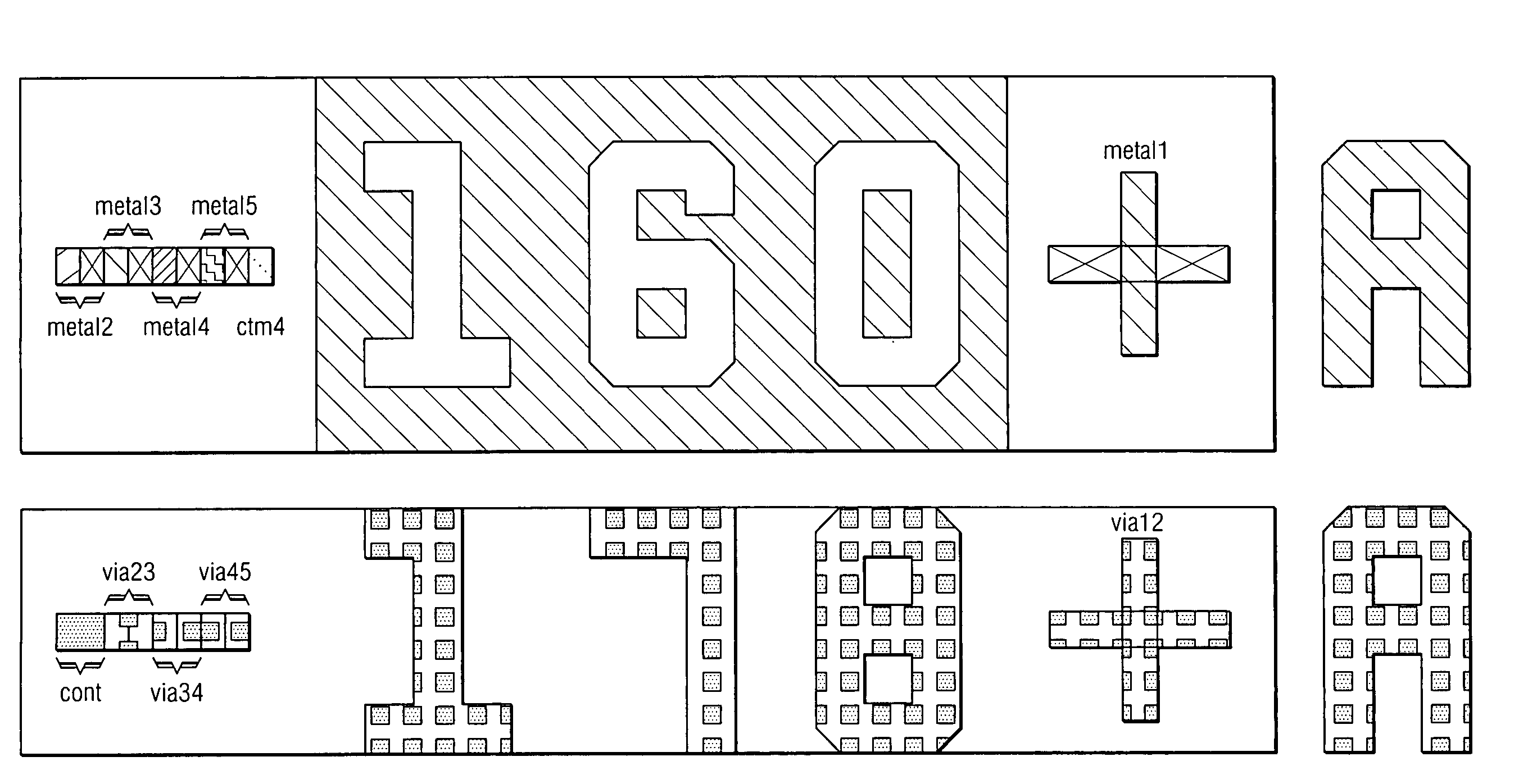
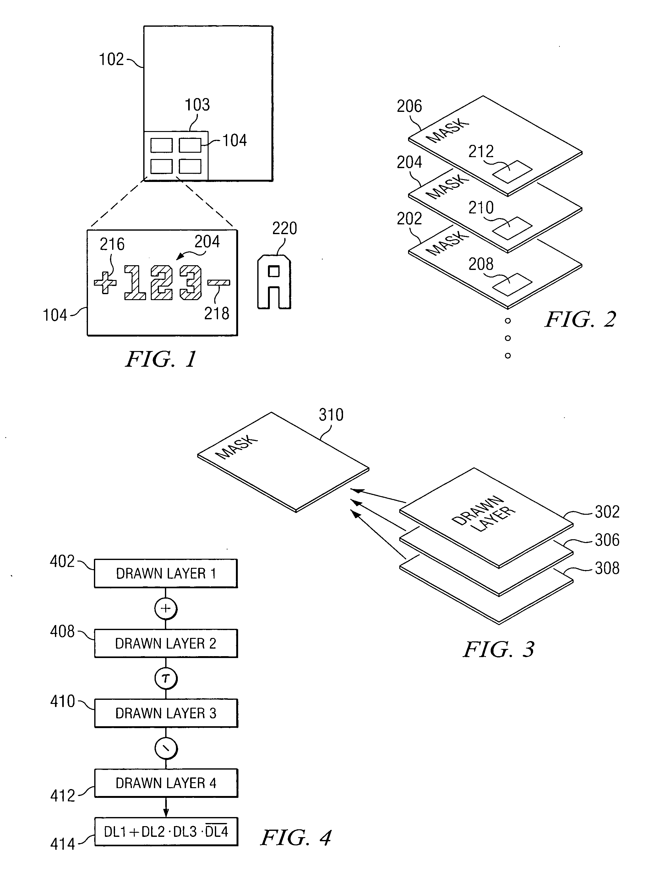
[0020] Referring now to FIG. 1, there is illustrated a diagrammatic view of an integrated circuit 102 that has circuitry formed on the surface thereof. This circuitry is formed through the use of a plurality of masks, each mask defining a processing step in the manufacturing process. The resulting integrated circuit will have disposed at the low corner thereof, in the disclosed embodiment, indications of various mask layers, in a region 103, there being a plurality of indicator regions 104 contained therein, each associated with a different mask level. This will be described herein below. These indicators at the mask level allow an observer to quickly ascertain from the indicators themselves information about the mask generation process and whether the manufacturer had in fact assembled the correct layout layers for each mask, from design data provided by the designer.
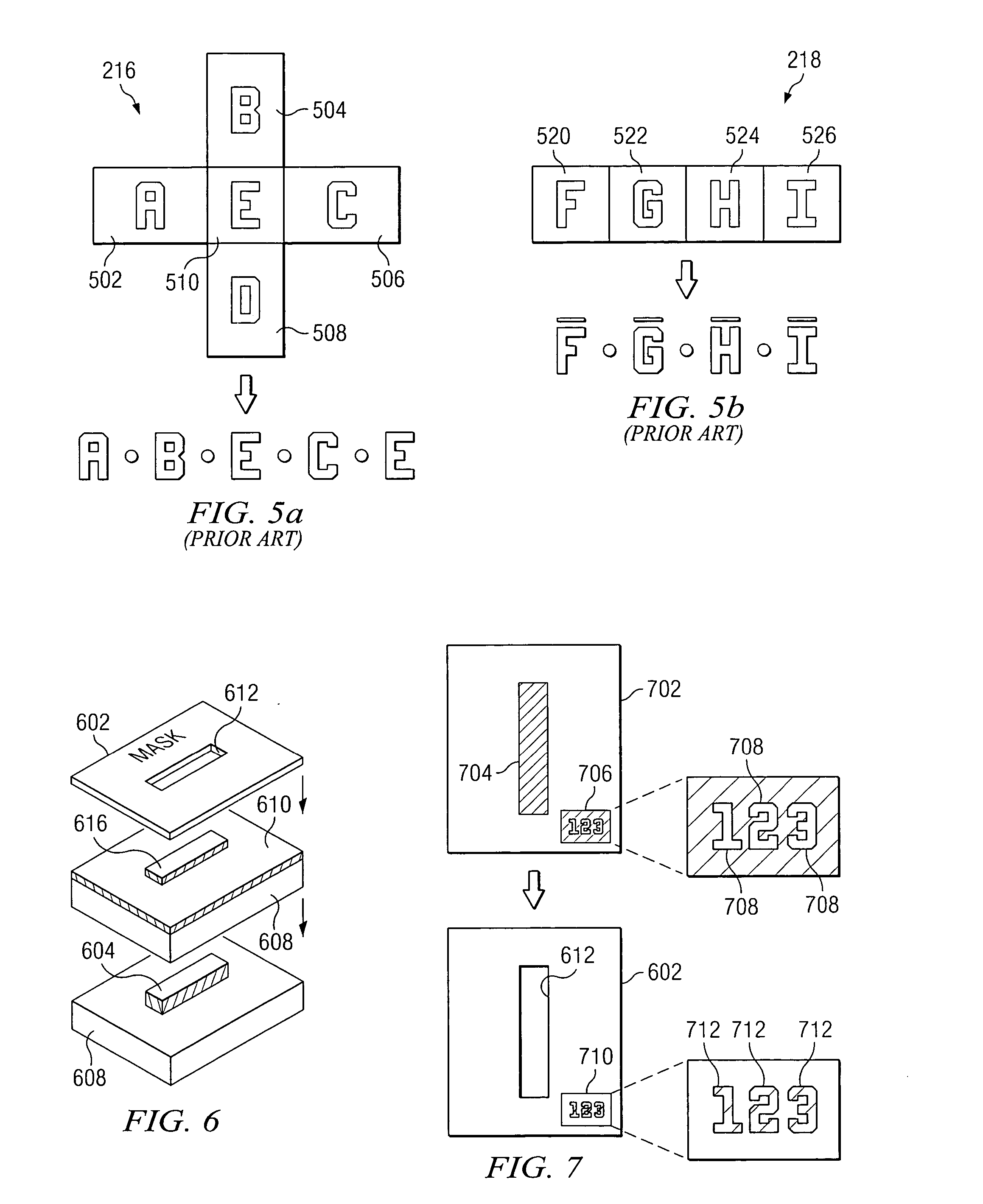
[0021] Referring now to FIG. 2, there is illustrated a diagrammatic view of the various mask layers that are provid...
PUM
 Abstract
Description
Claims
Application Information