Bump for semiconductor package, semiconductor package applying the bump, and method for fabricating the semiconductor package

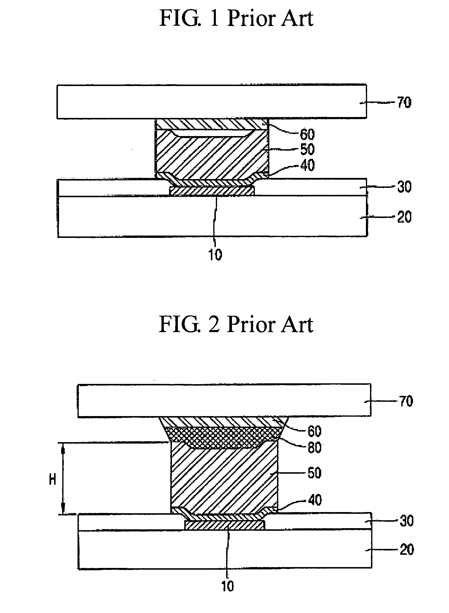
a semiconductor and package technology, applied in the field of semiconductor package bumps, can solve the problems of difficult to reduce the size of lines and electrode terminals, the disadvantage of conventional semiconductor packages in slim and lightweight shapes, and the need for a long time for wire bonding, etc., to achieve excellent electrical properties and high reliability.

Inactive Publication Date: 2005-10-13
NEPES CO LTD
View PDF4 Cites 63 Cited by
  • Summary
  • Abstract
  • Description
  • Claims
  • Application Information

AI Technical Summary

Benefits of technology

[0022] Therefore, an object of the present invention is to provide a bump for a semiconductor package which can electrically connect electrode terminals of a PCB to electrode pads

Problems solved by technology

In addition, wire bonding requires a long time, which is disadvantageous in a slim and lightweight shape and a mass production.
It is this difficult to reduce a size of lines

Method used


Image

  • Bump for semiconductor package, semiconductor package applying the bump, and method for fabricating the semiconductor package
  • Bump for semiconductor package, semiconductor package applying the bump, and method for fabricating the semiconductor package
  • Bump for semiconductor package, semiconductor package applying the bump, and method for fabricating the semiconductor package

Examples


Embodiment Construction

[0034] Reference will now be made in detail to the preferred embodiments of the present invention, examples of which are illustrated in the accompanying drawings.

[0035] A bump for a semiconductor package, a semiconductor package applying the bump, and a method for fabricating the semiconductor package in accordance with the preferred embodiments of the present invention will now be described in detail with reference to the accompanying drawings.

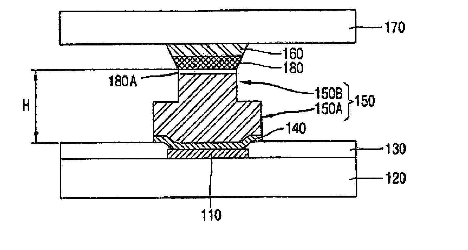
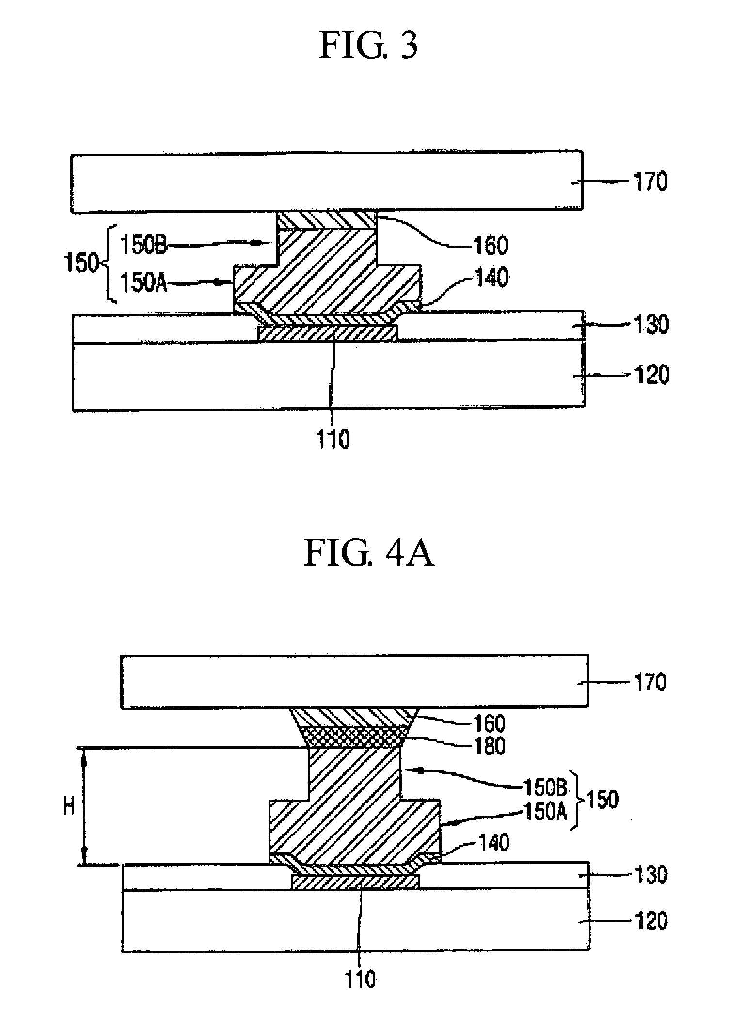
[0036]FIG. 3 is an exemplary diagram illustrating a semiconductor package using a metal bump in accordance with the present invention.

[0037] As shown in FIG. 3, the semiconductor package includes a semiconductor chip 120 on which an electrode pad 110 has been formed, a protecting film 130 formed on the surface of the semiconductor chip 120, for selectively exposing the electrode pad 110, a metal adhering layer 140 formed on the electrode pad 110, and extended from the upper portion of the electrode pad 110 to the upper portion of the prote...


PUM

PropertyMeasurementUnit
Grain sizeaaaaaaaaaa
Temperatureaaaaaaaaaa
Widthaaaaaaaaaa

Abstract

The present invention discloses a bump for a semiconductor package, a semiconductor package applying the bump, and a method for fabricating the semiconductor package. As a second bump unit contacting an electrode terminal of a PCB has a smaller width than a first bump unit contacting an electrode pad of a semiconductor chip through a metal adhering layer, even if a pitch between the electrode pads of the semiconductor chip does not correspond to the pitch between the electrode terminals of the PCB, contact reliability is improved by the bump. In addition, the bump does not contact lines adjacent to the electrode terminal of the PCB, thereby preventing a mis-operation of the semiconductor package. Accordingly, the pitch between the electrode pads of the semiconductor chip and the pitch between the bumps can be minimized.

Description

CROSS REFERENCE TO RELATED APPLICATIONS [0001] This U.S. non-provisional application claims priority under 35 U.S.C. § 119 to Korean Patent Application No. 2004-24217 filed Apr. 8, 2004, the contents of which are incorporated by reference.BACKGROUND OF THE INVENTION [0002] 1. Field of the Invention [0003] The present invention relates to a bump for a semiconductor package, a semiconductor package applying the bump, and a method for fabricating the semiconductor package. [0004] 2. Description of the Background Art [0005] In general, a semiconductor package fabricated by wire boding is larger in size than a semiconductor chip because electrode terminals of a printed circuit board (PCB) and electrode pads of the semiconductor chip are electrically connected by a conductive wire. In addition, wire bonding requires a long time, which is disadvantageous in a slim and lightweight shape and a mass production. [0006] According to high integration, high performance and high speed tendencies o...

Claims


Application Information

Patent Timeline
IPC IPC(8): H01L23/485H01L23/48H01L21/60
CPCH01L24/02H01L24/03H01L24/11H01L24/16H01L24/83H01L2224/03912H01L2224/0401H01L2224/11472H01L2224/11474H01L2224/13099H01L2224/13111H01L2224/13144H01L2224/13147H01L2224/16H01L2224/29111H01L2224/83851H01L2924/01006H01L2924/01013H01L2924/01015H01L2924/01022H01L2924/01029H01L2924/0103H01L2924/01047H01L2924/0105H01L2924/01074H01L2924/01078H01L2924/01079H01L2924/01082H01L2924/014H01L2924/01023H01L2924/01024H01L2924/01033H01L2924/00014H01L2924/07811H01L2924/00H01L2224/13017H01L24/13H01L24/05D21H17/65D21H21/36D21H27/20
Inventor YEO, YONG-WOON
Owner NEPES CO LTD
Why Eureka
Try Eureka