Display device and its driving method

Active Publication Date: 2005-10-13
SOLAS OLED LTD
View PDF14 Cites 41 Cited by
  • Summary
  • Abstract
  • Description
  • Claims
  • Application Information

AI Technical Summary

Benefits of technology

[0036] Thus, according to the present invention, in the display device that controls the optical elements using the current designation system, it is

Problems solved by technology

However, the display device with the aforementioned various kinds of pixel drive circuits in the display pixel has the following problems.
Namely, the pixel drive circuit using the voltage drive system as illustrated in FIG. 11A has the problem in that when device characteristics of two thin-film transistors Tr 11 and Tr12 such as a channel resistance, and the like are changed by ambient temperature, variation with the passage of time, and the like, this exerts an influence upon the drive current supplied to the light-emitting devices to make it difficult to realize a predetermined light-emitting characteristic stably for a long time.
Moreover, there is a problem in that when each of the display pixels that forms the display panel is made finer to improve high definition of the display image quality, a variation in the operation characteristic such as source-drain current of each of the thin-film transistors Tr11 and Tr12 that forms the pixel drive circuit increases, so that appropriate gray-scale control cannot be performed and a variation in the display characteristic of each display pixel occurs, causing deterioration in the image quality.
In this case, when amorphous silicon is used, the PMOS transistor with the sufficient operation characteristic and function cannot be formed.
However, the manufac

Method used


Image

  • Display device and its driving method
  • Display device and its driving method
  • Display device and its driving method

Examples


Example

BEST MODE OF CARRYING OUT THE INVENTION

[0048] The following will explain the details on the display device and the display device driving method according to the present invention based on the embodiment illustrated in the drawings.

[0049] First of all, an explanation will be given of the general structure applied to the display device according to the present invention with reference to the drawings.

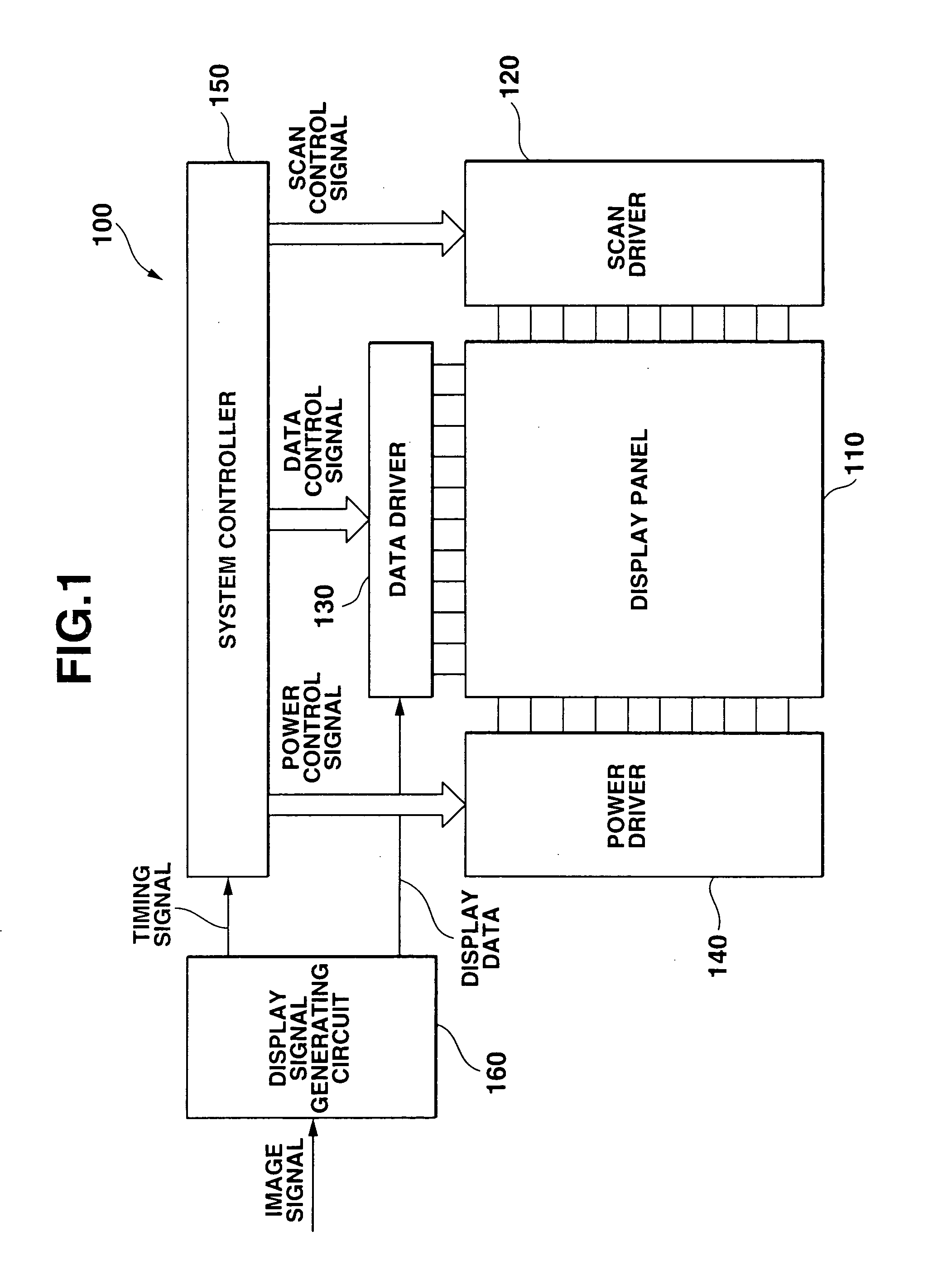
[0050]FIG. 1 is a schematic block diagram illustrating one example of the general structure of a display device according to the present invention.

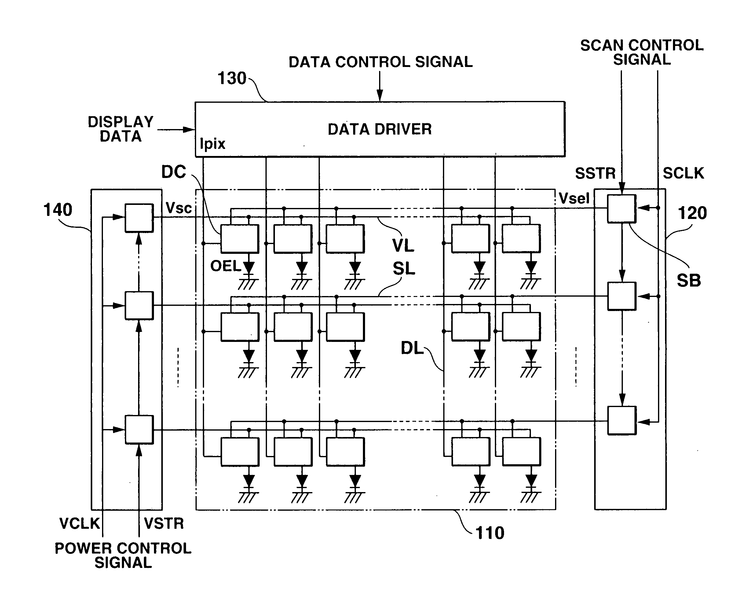
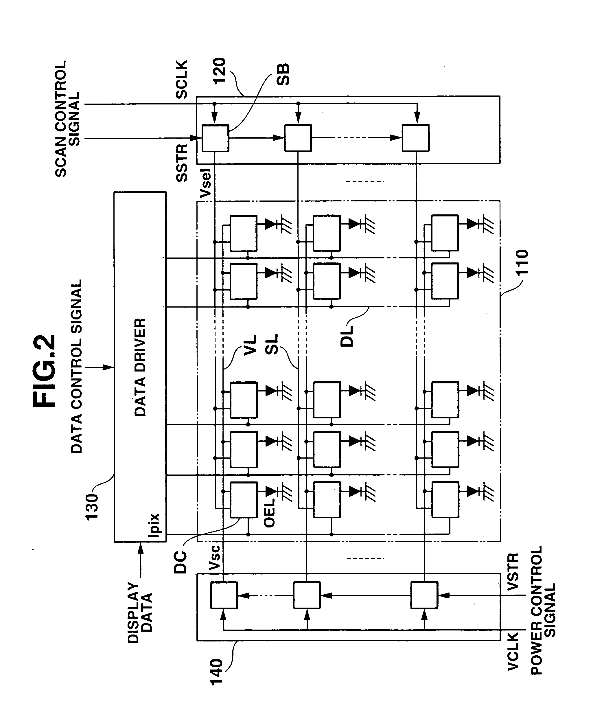
[0051]FIG. 2 is a schematic diagram illustrating one example of a display panel applied to the display device according to the present embodiment. Hereinafter, the same components as those of the aforementioned prior art will be explained using the same reference numerals as those of the aforementioned prior art added to the same components as those thereof.

[0052] As illustrated in FIG. 1 and FIG. 2, a display device 100 according to the ...


PUM


Abstract

A display panel (110) comprises a plurality of optical elements (OEL) each having a pair of electrodes and performing an optical operation according to current passing between the pair of electrodes, a current line (DL), a switch circuit (Tr2) that passes a write current (Ia) with a predetermined current value through the current line (DL) during a selection time (Tse) and stops passing current during a non-selection time (Tnse), and a current storage circuit (Tr1, Tr2, Cs, Cp) that stores current data according to the current value of the write current (Ia) passing through the current line (DL) during the selection time (Tse) and that supplies a drive current (Ib) having a current value, which is obtained by subtracting a predetermined offset current (Ioff) from the current value of the stored write current (Ia), to the optical elements (OEL) during the non-selection time (Tnse). The current storage circuit (Tr1, Tr2, Cs, Cp) includes a first capacitor device (Cs) to which an electrical charge corresponding to the write current (Ia) is written and a second capacitor device (Cp) to which an electrical charge corresponding to offset current (Ioff) is written, and the second capacitor device (Cp) has a capacitive value, which is equal to or larger than the first capacitor device (Cs).

Description

TECHNICAL FIELD [0001] The present invention relates to a display device and a driving method for the display device and particularly to a display device having a display panel with arrangements of a plurality of optical elements that emit light with a predetermined luminance gray-scale by supplying current in accordance with an image signal, and a driving method for the display device. BACKGROUND ART [0002] Conventionally, there has been known a light-emitting type display device having a display panel in which organic electroluminescence devices (hereinafter referred to as “organic EL devices”), inorganic electroluminescence elements (hereinafter referred to as “inorganic EL devices”) or self-luminous light emitting devices (optical elements) such as light-emitting diodes (LEDs) and the like are arranged in a matrix form. [0003] Particularly, the light-emitting type display device using an active matrix drive system has higher display response speed than the liquid crystal display...

Claims


Application Information

Patent Timeline
IPC IPC(8): H01L51/50G09G3/00G09G3/20G09G3/30G09G3/32H05B33/14
CPCG09G3/325G09G2300/0417G09G2300/0819G09G2300/0847G09G2320/043G09G2300/0866G09G2310/027G09G2320/0223G09G2300/0852G09G3/30G09G3/32
Inventor YAMADA, HIROYASUTAKEI, MANABU
Owner SOLAS OLED LTD
Why Eureka
Try Eureka